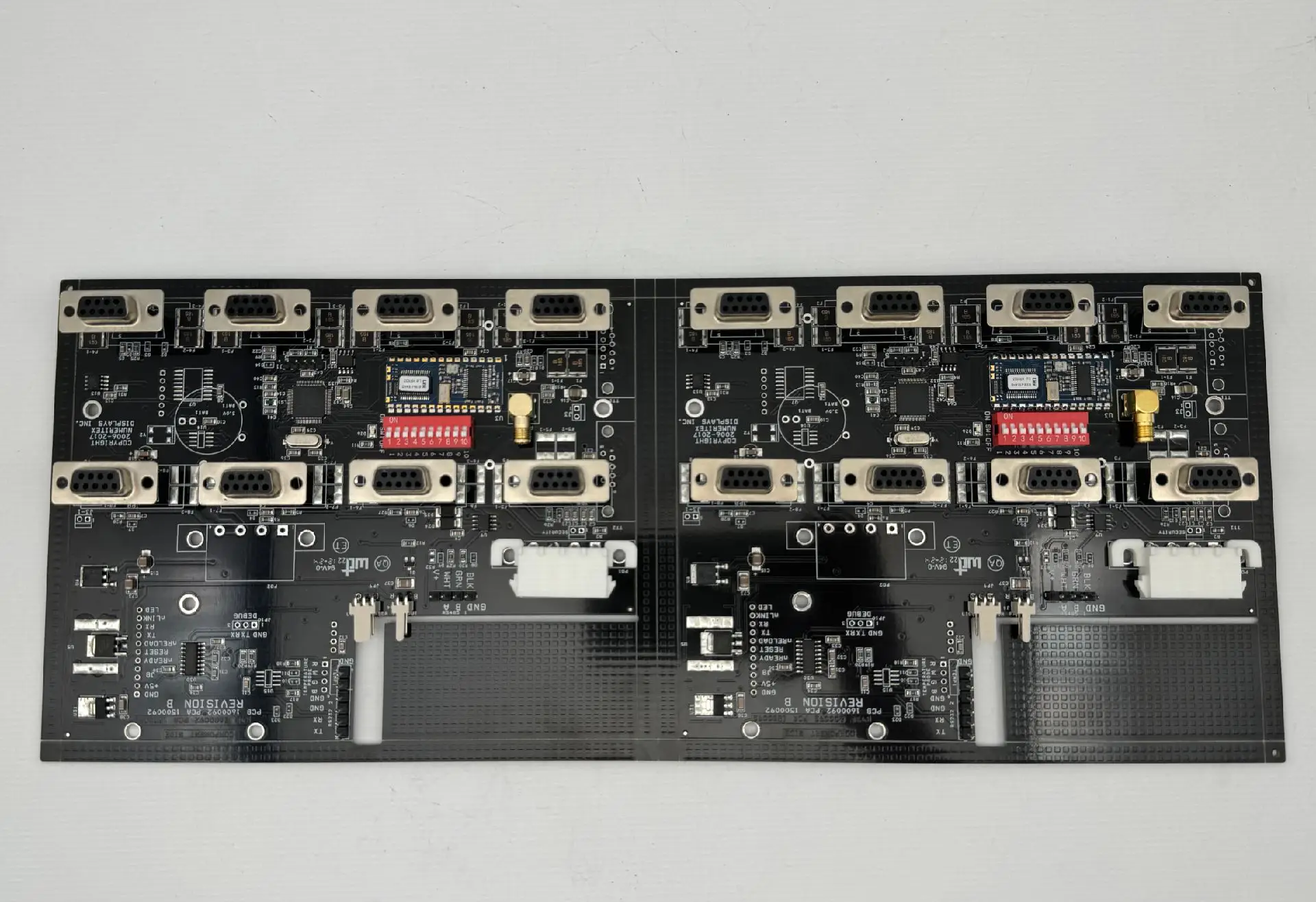
From Design to Mass Production: 7 Common Pitfalls Engineers Encounter in PCB/PCBA Manufacturing and Their Solutions
As a company specializing in PCB manufacturing and PCBA assembly, we handle a large number of design files from hardware engineers in our daily work and have dealt with many process issues that emerge during the transition from prototyping to mass production. Many problems appear fine during the layout stage, but once SMT mass production begins, they erupt in clusters: impedance deviation, BGA cold solder joints, QFN bottom voids, components falling off after depanelization, board warpage, delamination, and more. The common characteristic of these problems is that the design stage does not fully consider the process boundaries of PCB manufacturing and PCBA assembly. This article, from the perspective of actual PCB production and PCBA manufacturing processes, outlines seven high-frequency and high-cost engineering problems and provides practical design recommendations.
1. Impedance Control: Don't Just Calculate Line Width; Stackup and Material Tolerances Are the Key
Many engineers calculate a differential impedance of 100Ω in software, but during prototype testing they find large impedance deviations and poor high-speed signal eye diagrams. The reason is often not the software, but the inconsistency between actual material parameters and the parameters used for calculation.
Manufacturing Recommendations:
1. For high-speed and RF boards, prioritize low-loss materials with a Dk tolerance of ±0.05, such as Panasonic M4/M6 grade low-loss materials or other high-performance laminates with a Dk tolerance of ±0.05, rather than standard FR-4.
2. During design, do not rely only on software default parameters. You must ask the board manufacturer to provide the actual stackup, including prepreg type, core thickness, copper thickness, and solder mask thickness.
3. Keep a complete reference plane below critical differential pairs and avoid crossing splits. For the solder mask above differential pairs, consider opening windows or using low-Dk solder mask ink.
4. When impedance control is required to ±5%, clearly mark it in the PCB files and require the board manufacturer to provide a TDR impedance test report, not just calculated values.
5. BGA with 0.5mm Pitch and Below: Solder Mask Dams and Pad Definition Determine Soldering Yield
For a 0.5mm pitch BGA, the pad center-to-center distance is only 0.5mm, the pad diameter is usually 0.25 to 0.3mm, and the gap between pads is only 0.2 to 0.25mm. If a solder mask dam is forced, the dam width is often less than 0.1mm, and the solder mask is prone to peeling or residue, which in turn causes soldering defects. If no solder mask dam is used, there is concern about solder bridging and short circuits.
Manufacturing Recommendations:
1. For BGAs with 0.5mm pitch and below, prioritize NSMD (non-solder mask defined) pads. The solder mask opening should be enlarged by 0.05 to 0.075mm per side beyond the pad to avoid solder mask encroaching on the pad.
2. If a solder mask dam is required, the minimum dam width must not be less than 0.1mm. When this cannot be guaranteed, it is better not to have a dam and instead reduce short circuit risk by optimizing stencil apertures and reflow profiles.
3. Vias in the BGA area must be resin-filled and plated flat, or use VIPPO (via-in-pad plated over) technology, to avoid solder beads trapped in vias and uneven pad surfaces that cause cold solder joints.
4. For pad surface finish, prioritize ENIG or OSP. HASL is not recommended because its poor surface planarity seriously affects BGA soldering yield.
5. Thermal Pads / Bottom Pads: Improper Via and Via Filling Design Leads to Frequent Voids and Cold Solder Joints
Devices such as QFNs, power MOSFETs, and LGAs usually have a large thermal pad on the bottom. If thermal vias on the PCB are not filled or are poorly filled, molten solder paste can flow through the vias, causing voids. Air inside the vias expands when heated and may also produce solder beads or even lift the component.
Manufacturing Recommendations:
1. Vias inside the thermal pad are recommended to have a diameter of 0.2 to 0.3mm and a pitch of 0.8 to 1.2mm, arranged in a matrix pattern, avoiding concentration at the center of the large pad.
2. The vias must be resin-filled or copper-filled and the surface must be plated flat to ensure the bottom pad forms a complete plane.
3. Do not open the entire stencil area. It is recommended to use a grid or diagonal stripe pattern, with coverage controlled at 40% to 60%, to reduce voids caused by large solder paste deposits.
4. Properly extend the soak zone in the reflow profile to allow the flux to fully volatilize, which can significantly reduce voiding.
5. Panelization and Depanelization: Improper V-Cut and Stamp Hole Design Causes Stress Damage to Components
Depanelization is an invisible killer that many engineers overlook. If the V-Cut residual thickness is too large, the depaneling machine requires greater force, and mechanical stress is directly transmitted to chip capacitors, resistors, and solder joints. If the residual thickness is too small, the board is prone to breakage during transportation and component placement. If stamp holes are too close to components, depanelization can also cause capacitor cracking or micro-cracks in solder joints.
Manufacturing Recommendations:
1. V-Cut residual thickness is generally about one third of the board thickness. For example, for a 1.6mm board, the residual thickness should be controlled around 0.5mm with a tolerance of ±0.1mm.
2. The distance from the V-Cut line to the edge of component pads should be at least 1mm, and at least 2mm to chip ceramic capacitors, to avoid stress damage during depanelization.
3. Stamp hole diameter is recommended to be 0.3 to 0.5mm, hole center distance 0.8 to 1.2mm, and bridge width 3 to 5mm. Avoid placing fragile components in the stamp hole area.
4. Reserve a 3 to 5mm process edge along the board. Fiducial marks should be at least 3mm from the board edge.
5. For large thin boards, rigid-flex boards, or high-value boards, CNC routing or laser depanelization is recommended instead of V-Cut to reduce stress risk.
6. Surface Finish Selection: More Expensive Is Not Always Better—How to Choose Among ENIG, OSP, Immersion Silver, and HASL?
Engineers often ask, "Is ENIG always the best?" The answer is not necessarily. Different surface finishes have different applicable scenarios. Choosing the wrong one directly affects soldering yield, cost, and storage life.
ENIG has a flat surface, good storage stability, and can withstand multiple reflows, but it has the risk of black pad and is relatively expensive. It is suitable for BGAs with 0.5mm pitch and below, QFNs, and gold fingers. OSP is low cost and flat, but has a short storage life and weak multiple reflow capability, suitable for ordinary SMT double-sided boards and fine-pitch boards. Immersion silver has good high-frequency performance, a flat surface, and good conductivity, but it is prone to sulfidation and requires moisture-proof storage, suitable for high-speed, RF, and high-frequency boards. HASL has good solderability and low cost, but the surface is not flat and is not suitable for fine pitch. It is suitable for power boards, coarse-pitch, and through-hole boards. Immersion tin has a flat surface and good solderability, but is prone to tin whiskers. It is suitable for some fine-pitch boards, but the application environment needs to be evaluated.
Manufacturing Recommendations:
1. When there are components with 0.5mm pitch or below, BGAs, or QFNs, prioritize ENIG or OSP.
2. For ENIG, the nickel layer should be 3 to 5μm and the gold layer 0.05 to 0.1μm. If the gold layer is too thick, it can easily cause gold embrittlement of solder joints; if too thin, protection is insufficient.
3. For OSP boards, it is recommended to complete component placement within 24 to 48 hours after opening the package to avoid oxidation.
4. Immersion silver boards need anti-sulfidation packaging and should avoid long-term exposure to sulfur-containing environments.
5. Stencil and Solder Paste: Insufficient Solder Volume or Short Circuits for Fine-Pitch Components
Soldering of components such as 0.4mm pitch QFNs, 0201, and 01005 requires extremely high precision in stencil apertures and solder paste printing. Insufficient aperture area ratio leads to insufficient solder and tombstoning; excessive aperture size leads to short circuits and solder beads.
Manufacturing Recommendations:
2. The area ratio (aperture area divided by aperture wall area) should be no less than 0.66, and the aspect ratio should be no less than 1.5; otherwise, solder paste release becomes difficult.
3. For 0.4mm pitch QFN pads, the recommended aperture width is 0.18 to 0.2mm, with the length extended outward by 0.05 to 0.1mm. The bottom thermal pad should use a grid pattern.
4. Use Type 4 solder paste for 0201 components or Type 5 for 01005 components. Complete placement within 2 hours after printing to avoid flux volatilization.
5. During production, regularly check stencil tension and keep it no less than 35N/cm. Clean aperture burrs and residual solder paste in a timely manner.
6. Materials and Heat Resistance: Delamination, Blistering, and Board Warpage Under Lead-Free Reflow
Lead-free reflow peak temperature is usually 245 to 250°C, while standard FR-4 laminates have a Tg of only 130 to 140°C. If the board is thick, has heavy copper, or has a high layer count, multiple reflow cycles can easily cause delamination, blistering, hole copper cracking, and board warpage.
Manufacturing Recommendations:
1. For lead-free processes, prioritize laminates with a Tg of no less than 170°C. For heavy copper boards and high-layer-count boards, a Tg of no less than 180°C or high Td materials are recommended.
2. Pay attention to the Z-axis CTE. Excessive Z-axis CTE can cause hole copper to crack during thermal cycling. High Tg materials usually have a lower Z-axis CTE and are more suitable for high-reliability applications.
3. When copper thickness is no less than 3oz or board thickness is no less than 2.4mm, confirm the lamination process with the board manufacturer to avoid blistering or delamination.
4. During design, keep copper distribution uniform and avoid large areas without copper or uneven copper coverage to reduce warpage. Add balancing copper blocks or process copper pads if necessary.
Conclusion
PCB/PCBA mass production problems are often not caused by a single factor, but by the combination of design, materials, and process. Many seemingly sudden failures actually have their roots in the design stage.
Only when design and manufacturing are aligned in both directions can drawings be consistently turned into good products.
Note: The above parameters are common industry reference values. Specific designs should be confirmed based on the actual process capabilities of the board manufacturer. If you are developing high-speed boards, BGA boards, high-layer-count boards, or encountering production issues such as impedance, cold solder joints, or delamination, please contact us for a free DFM review to identify process risks in advance.