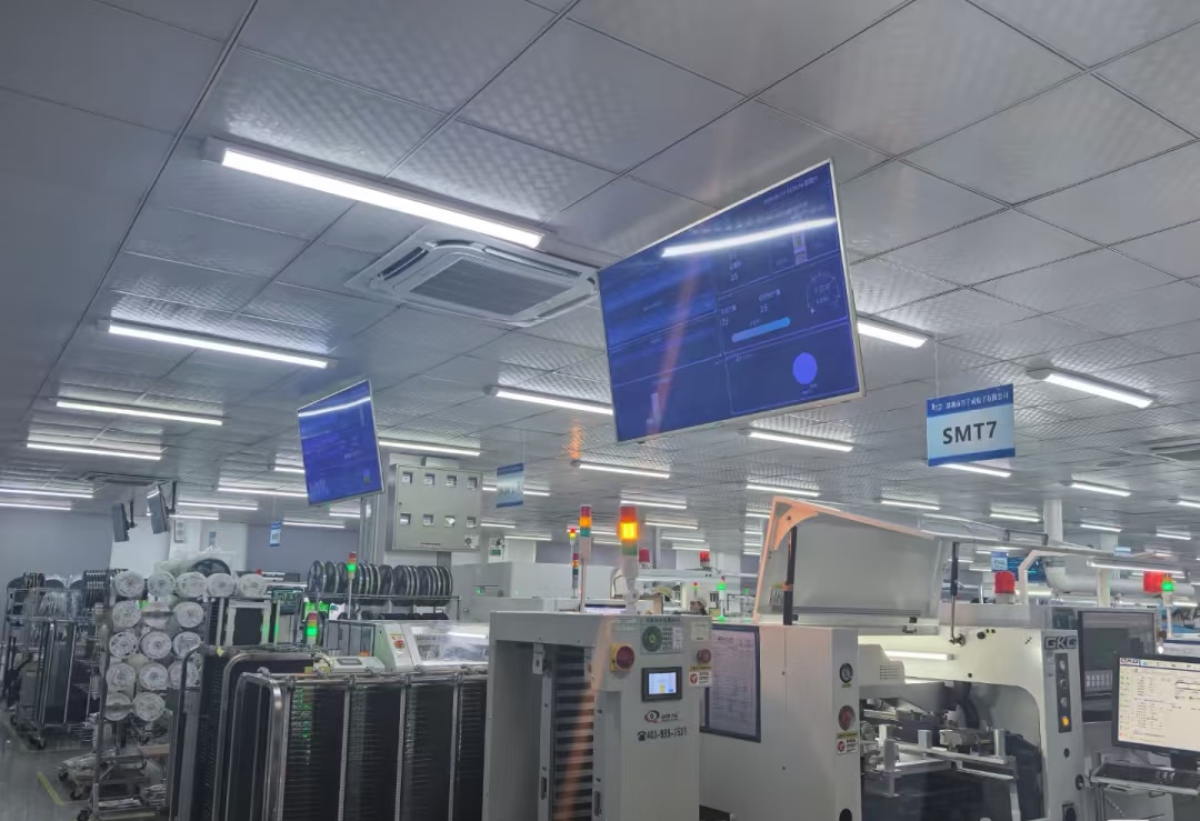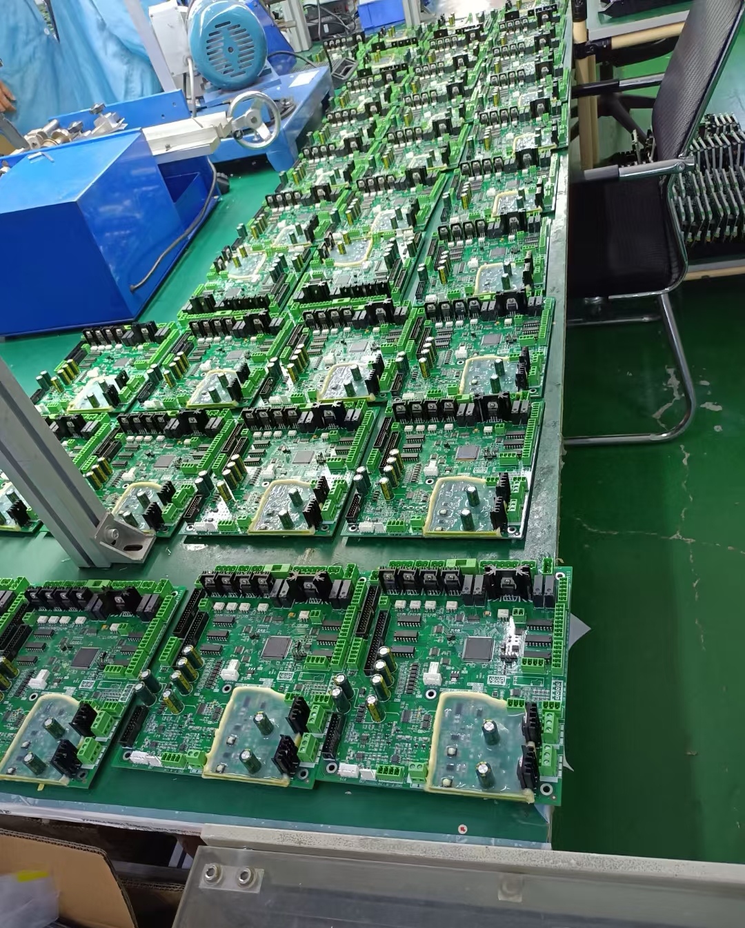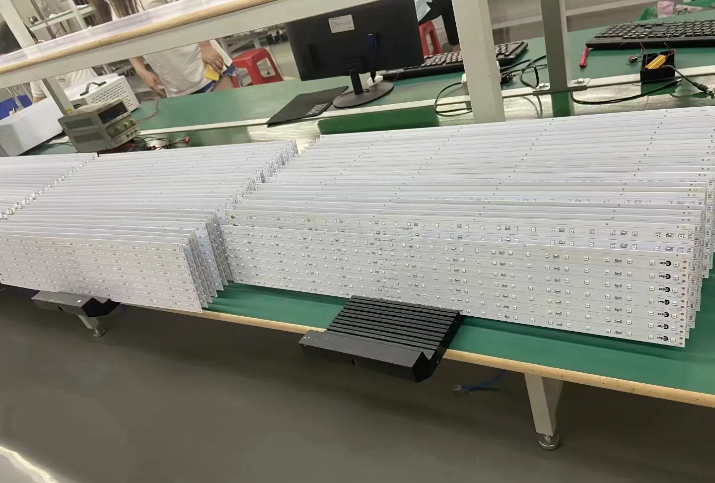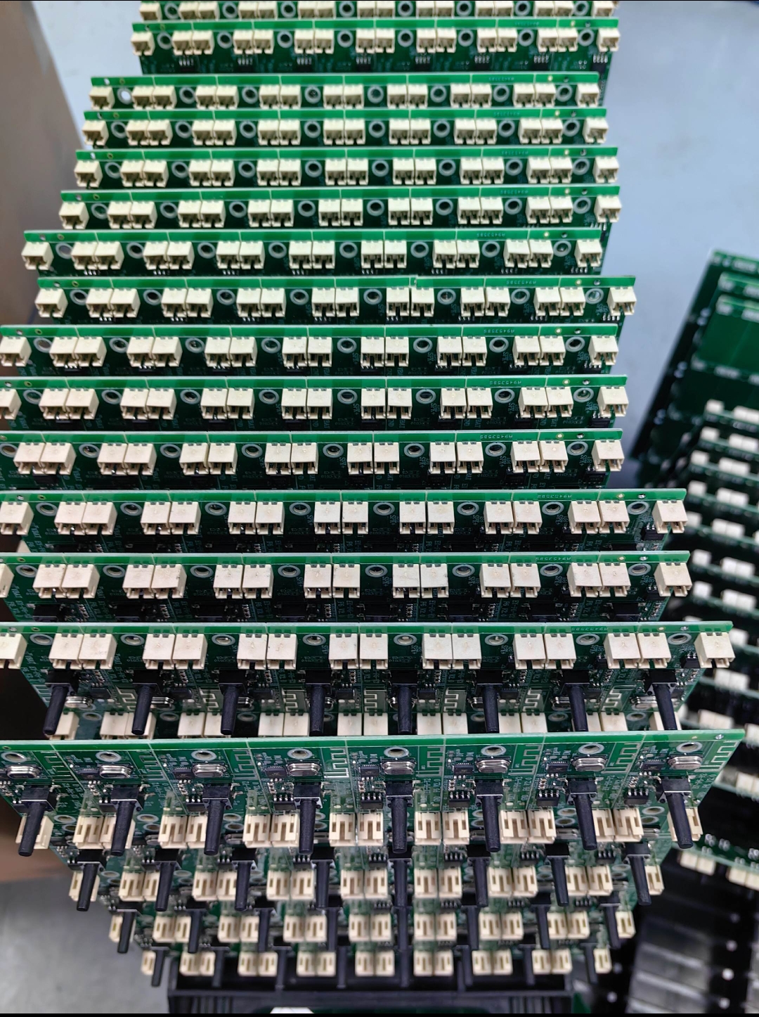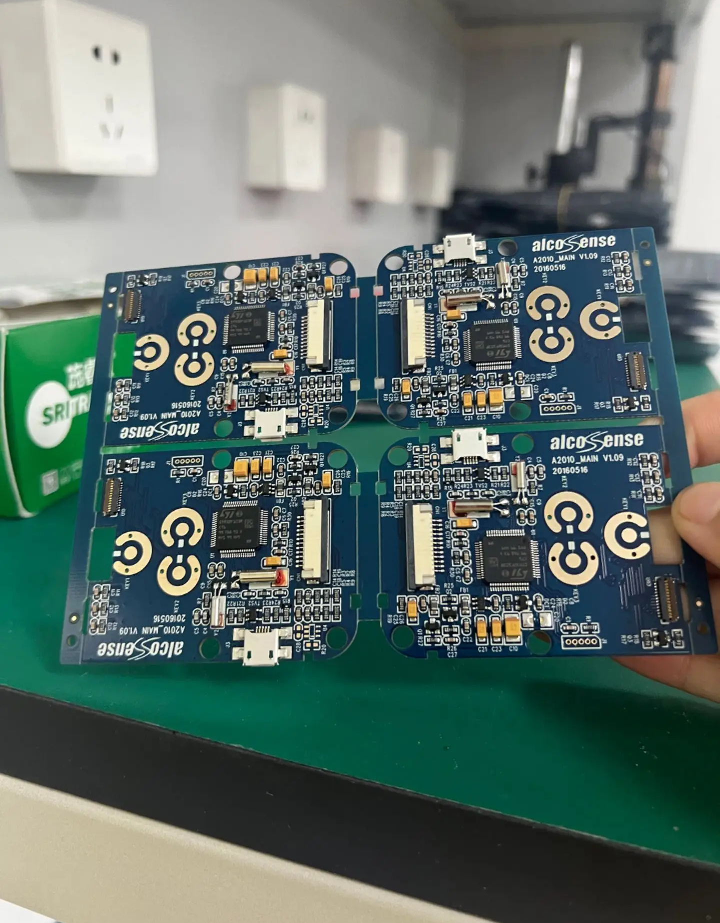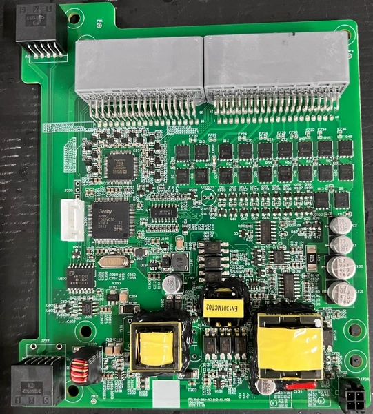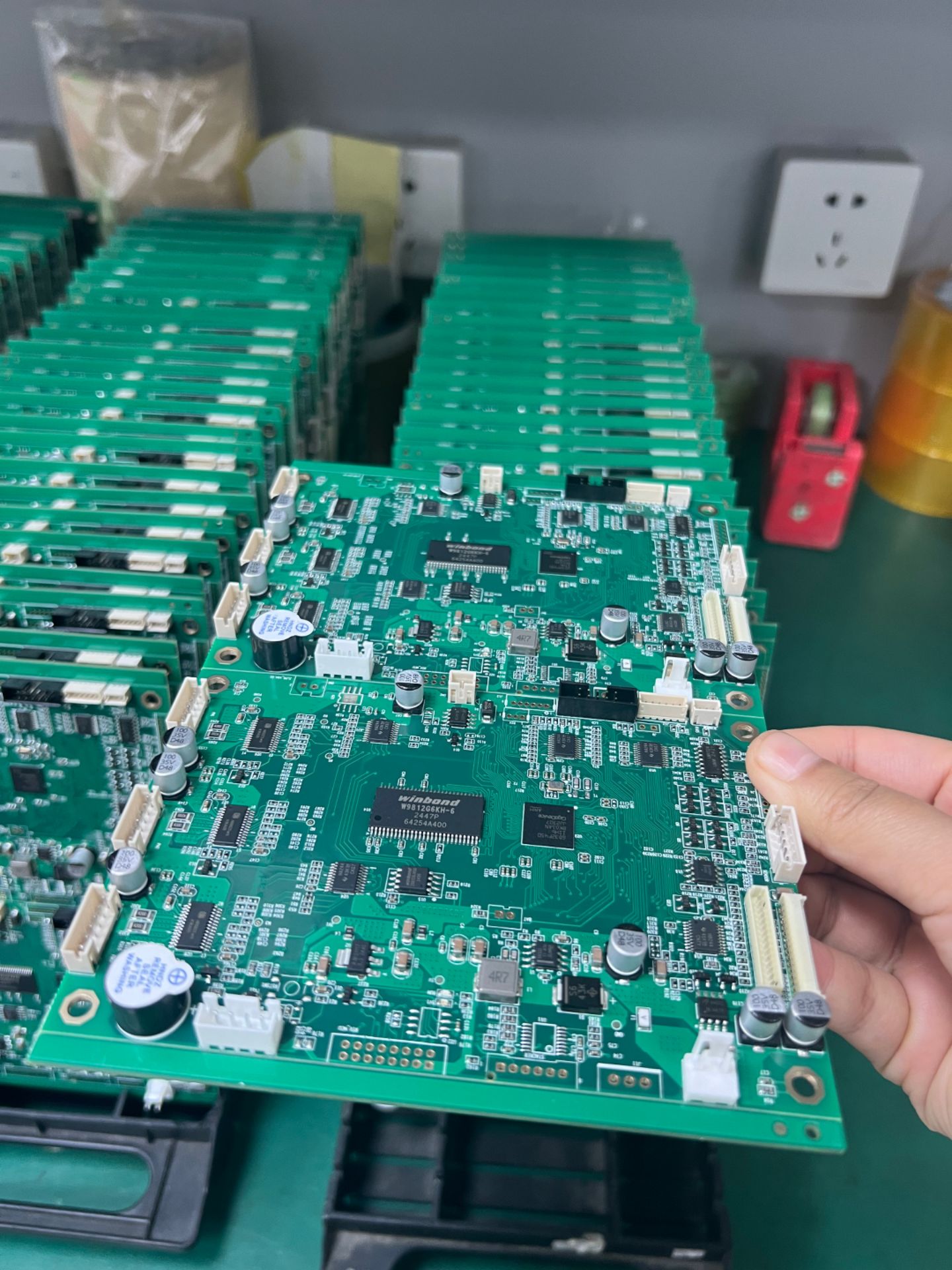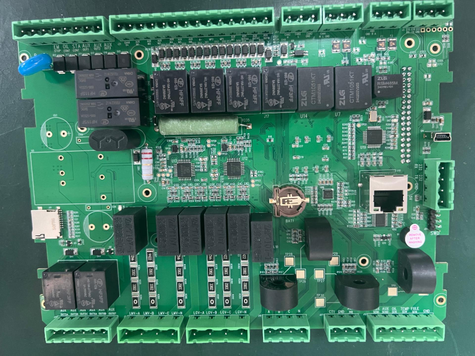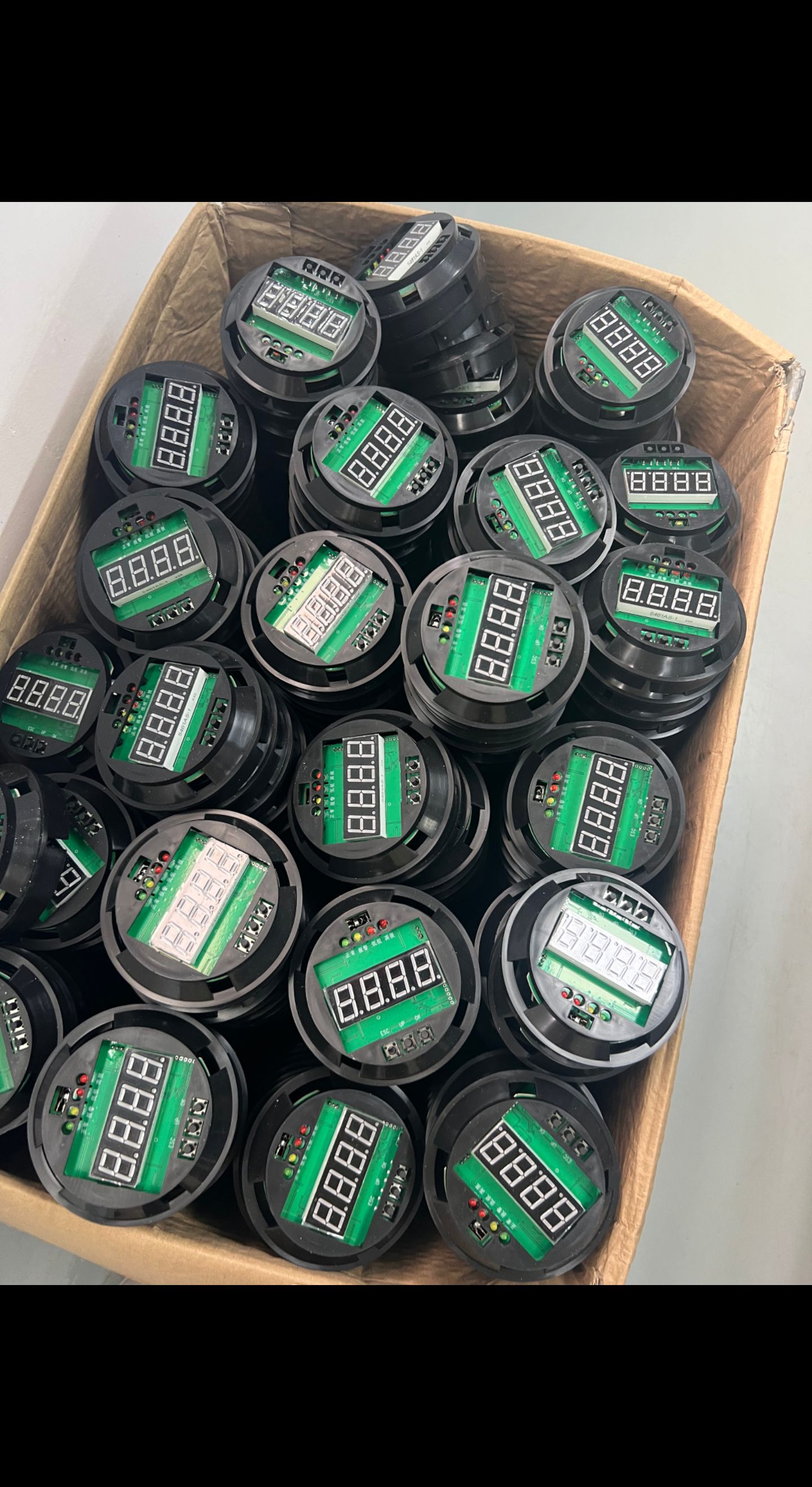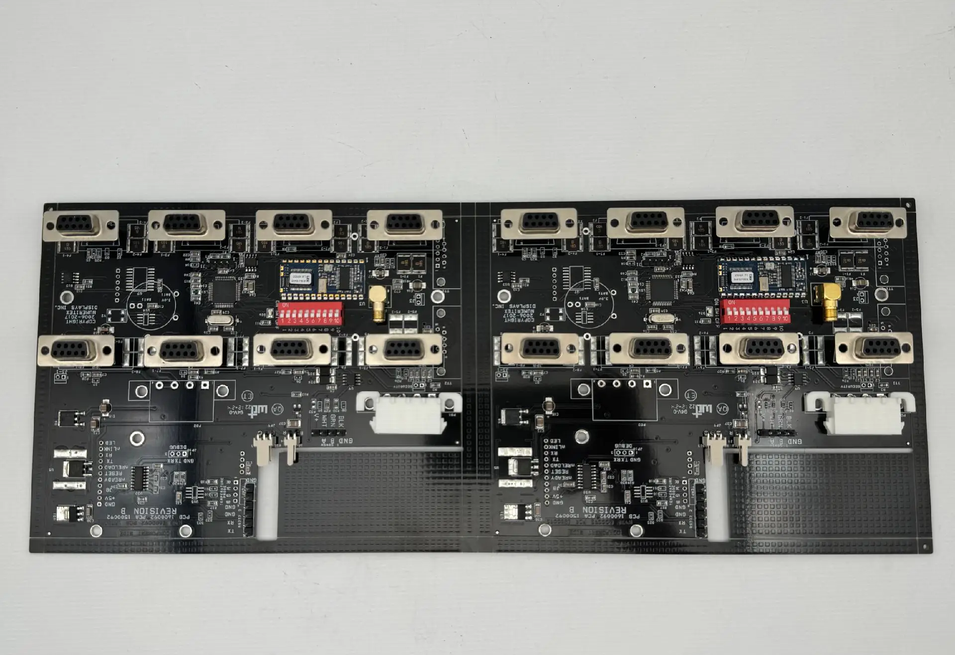
If you’re sourcing PCB fabrication or turnkey PCBA services from China, understanding the PCB manufacturing process helps you evaluate suppliers, communicate your requirements clearly, and avoid costly mistakes. In this guide, we walk through the key stages of printed circuit board production — from receiving your Gerber files to final electrical testing and packaging.
1. Design Review and DFM Check
Before production begins, a professional PCB manufacturer will run a Design for Manufacturability (DFM) check on your Gerber files, drill files, and Bill of Materials (BOM). This step identifies potential issues such as:
Trace width and spacing below the factory’s minimum capability
Annular ring violations
Missing solder mask openings
Unclear layer stack-up or material specification
Component placement conflicts for PCBA
A thorough DFM report helps prevent delays and ensures your board can be manufactured reliably at scale. At our factory, we provide free DFM feedback within 24 hours for all PCB and PCBA orders.
2. Material Preparation and Inner Layer Imaging
For multilayer PCBs, production starts with cutting the core material — typically FR-4, high-Tg FR-4, aluminum, or Rogers for high-frequency applications. The inner layers are coated with a photosensitive dry film, then exposed to UV light through a photomask created from your Gerber data.
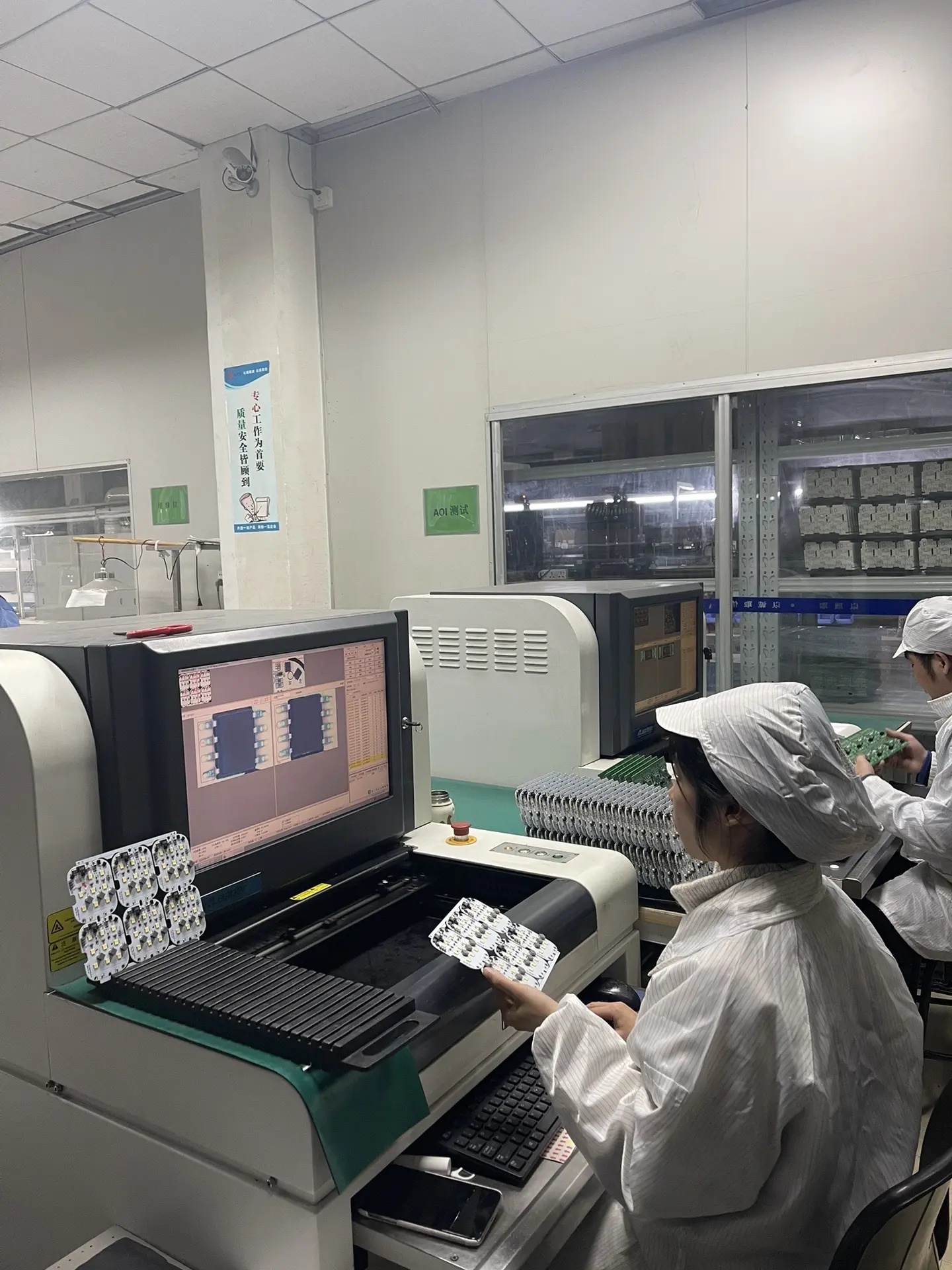
After exposure, the unexposed areas are developed away, leaving a pattern of copper traces. The exposed copper is then etched, and the remaining dry film is stripped. Automated Optical Inspection (AOI) is used to compare the inner layer patterns against the original design data, catching shorts, opens, or etching defects early.
3. Lamination and Drilling
The inner layers are stacked with prepreg (glass fiber impregnated with resin) and copper foil, then laminated under high temperature and pressure to form a solid multilayer board. After lamination, the panel goes through a baking process to remove moisture and stabilize dimensions.
Next, CNC drilling machines create holes for vias, through-hole components, and mounting. For high-density designs, laser drilling may be used for microvias in HDI boards. After drilling, the holes are deburred and cleaned to prepare for copper plating.
4. Electroless Copper and Plating
To make the drilled holes conductive, the entire panel undergoes electroless copper deposition, which coats the hole walls with a thin layer of copper. This is followed by electrolytic copper plating to build up the required copper thickness — typically 20–25 µm for standard boards, or more for high-current applications.
5. Outer Layer Imaging and Etching
The outer layers are imaged using the same photolithography process as the inner layers. After developing, the unwanted copper is etched away, leaving the final circuit pattern on the top and bottom surfaces. The panel is then plated with tin or another etch resist to protect the copper traces during etching.
6. Solder Mask and Silkscreen
Solder mask — usually green, but available in red, blue, black, white, or yellow — is applied to the entire board surface. It insulates the copper traces, prevents solder bridges during assembly, and protects the board from environmental damage. The solder mask is photo-imaged to expose pads and vias that need to remain accessible.
After solder mask application, the silkscreen layer is printed on top. This includes component outlines, reference designators, logos, and other markings that help during PCBA assembly and troubleshooting.
7. Surface Finish Application
The exposed copper pads must be coated with a surface finish to prevent oxidation and ensure good solderability. Common options include:
HASL (Hot Air Solder Leveling) — economical, widely used for through-hole and basic SMT
ENIG (Electroless Nickel Immersion Gold) — flat surface, excellent for fine-pitch components and long shelf life
OSP (Organic Solderability Preservative) — low-cost, RoHS-compliant, good for single-sided reflow
Immersion Silver / Tin — alternatives for high-frequency or press-fit applications
The choice depends on your design, assembly process, and budget. Our engineers can recommend the best surface finish for your application.
8. Electrical Testing and Inspection
Every board must pass electrical testing to verify continuity and isolation. The most common method is flying probe testing for prototypes and small batches, while dedicated fixtures (bed-of-nails) are used for mass production to reduce cost and increase speed.
In addition to electrical testing, visual inspection is performed according to IPC-A-600 standards. For PCBA orders, we also offer Automated Optical Inspection (AOI), X-ray inspection for BGA and QFN packages, and functional testing based on your test plan.
9. Profiling and Packaging
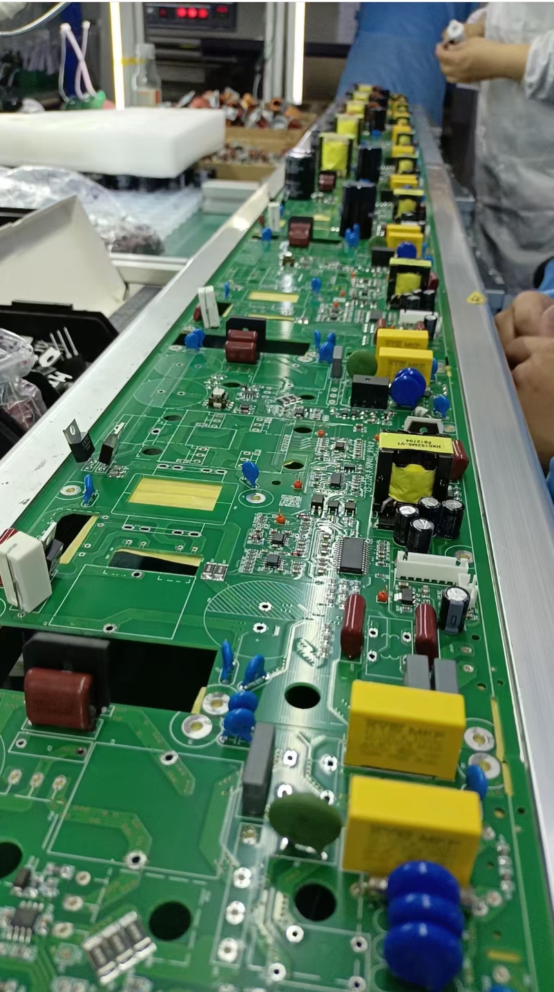
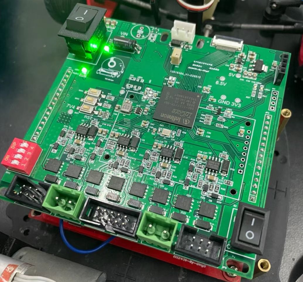
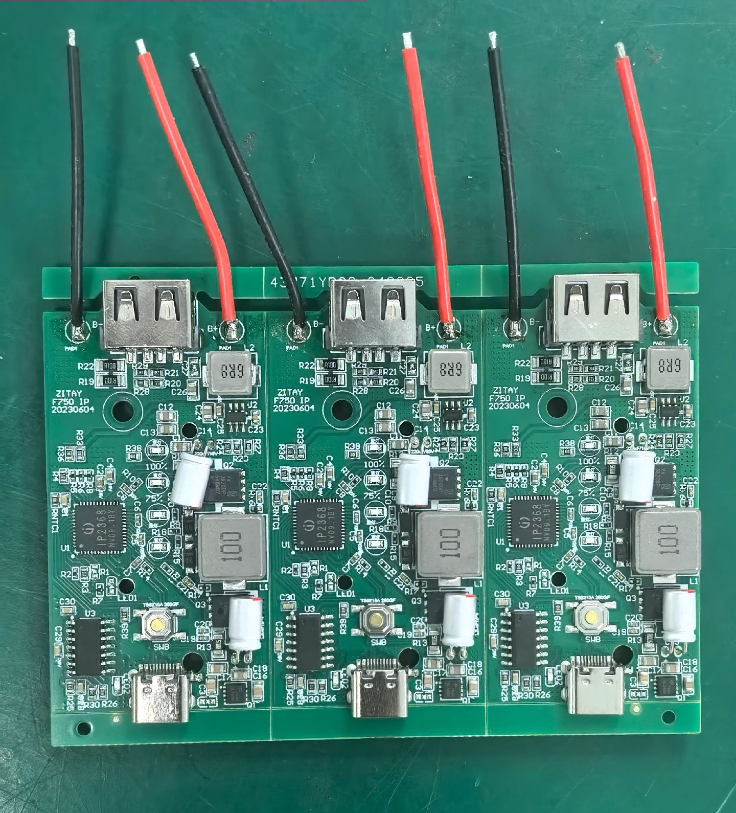
Finally, the boards are routed or V-scored from the production panel to their final shape. For PCBA, components are assembled either by SMT (Surface Mount Technology), through-hole, or mixed technology, followed by reflow soldering, wave soldering, or selective soldering.
After cleaning and final inspection, boards are vacuum-sealed with desiccant and humidity indicator cards, then packed in anti-static bags and sturdy cartons for safe international shipping.
Why Choose Us for PCB Fabrication and PCBA?
We are an ISO 9001-certified manufacturer with over 10 years of experience serving customers in Europe, North America, and Australia. We provide:
Prototype to mass production — no minimum order quantity for PCB prototypes
Turnkey PCBA service with full BOM sourcing
Free DFM and DFA feedback within 24 hours
UL, RoHS, and REACH compliance
DHL, FedEx, and UPS shipping with fast turnaround
If you’re looking for a reliable PCB and PCBA partner in China, contact us today with your Gerber files and BOM for a free quote.