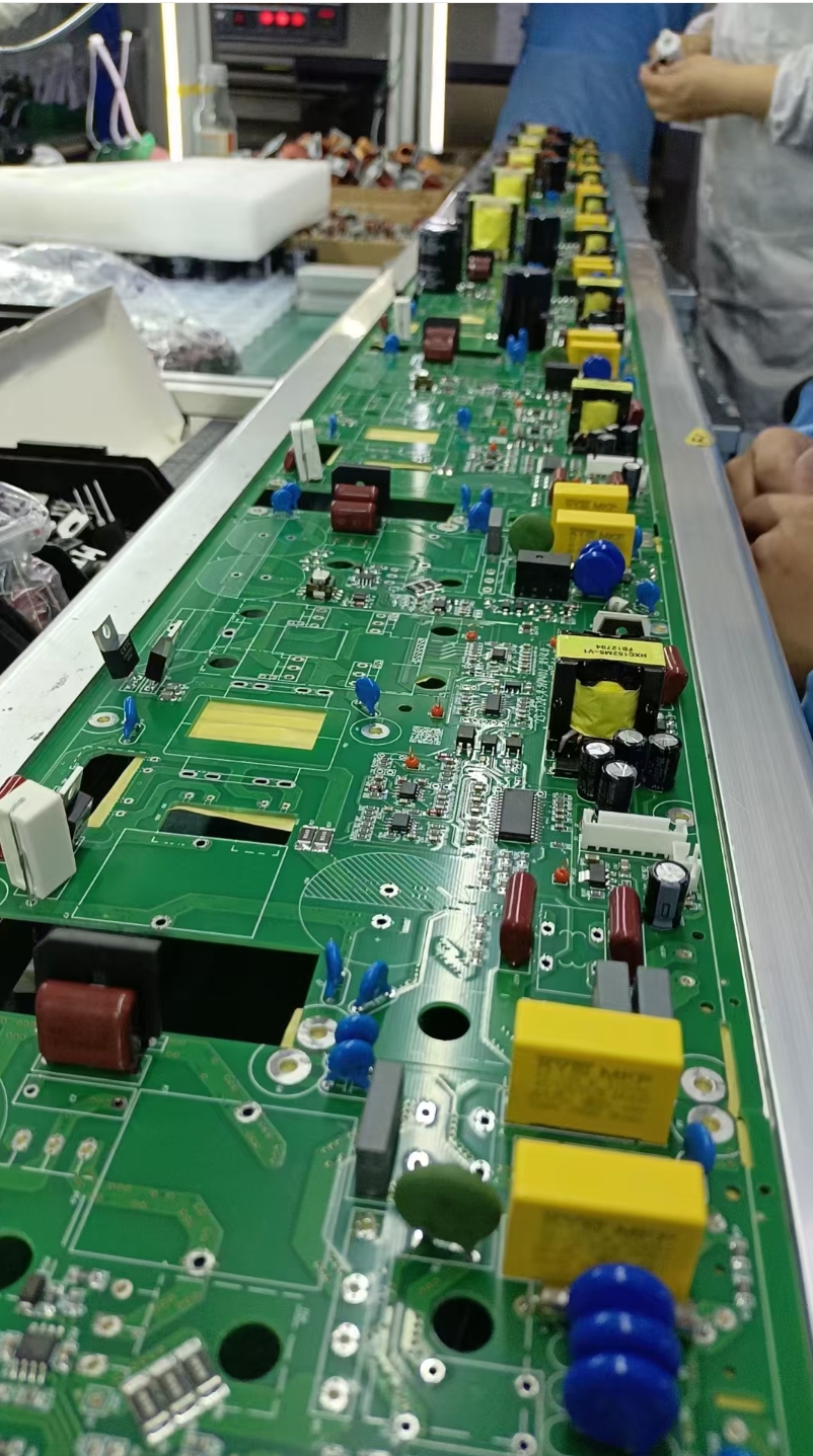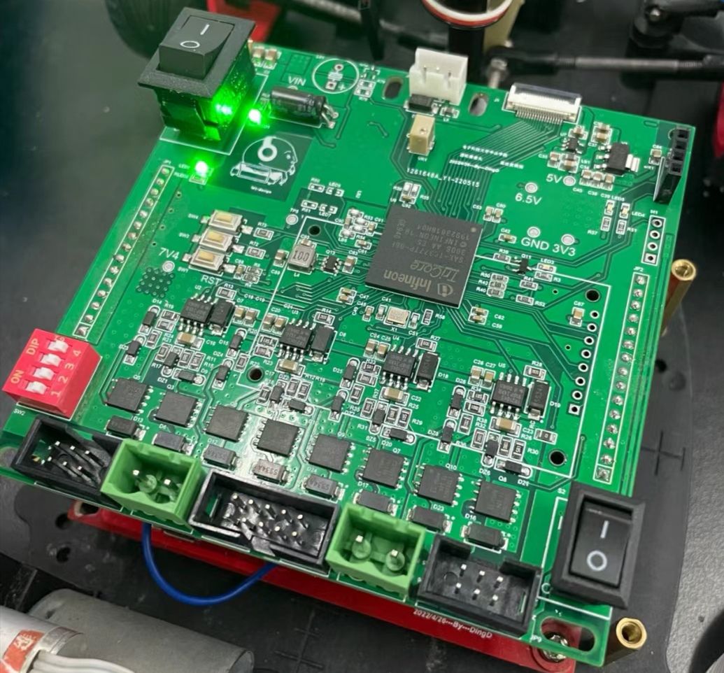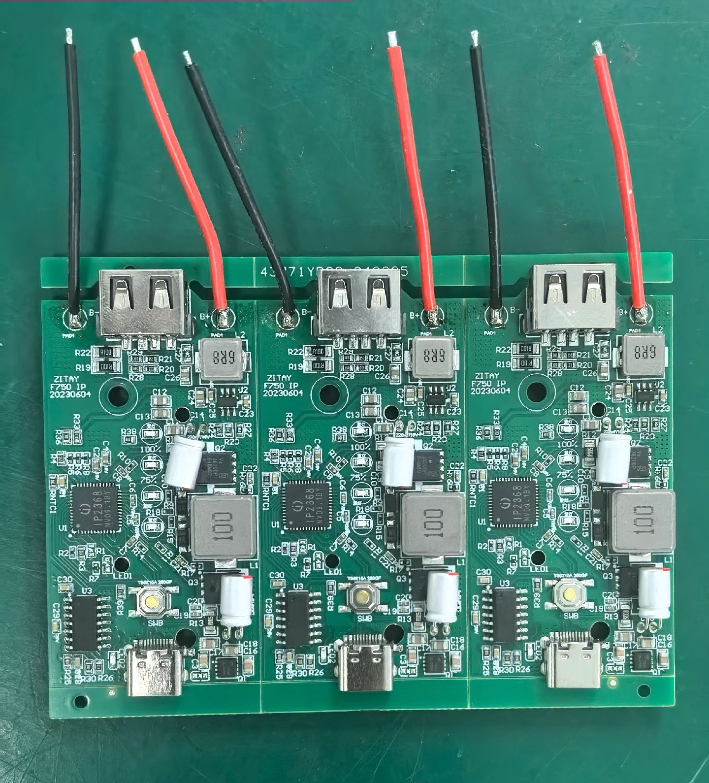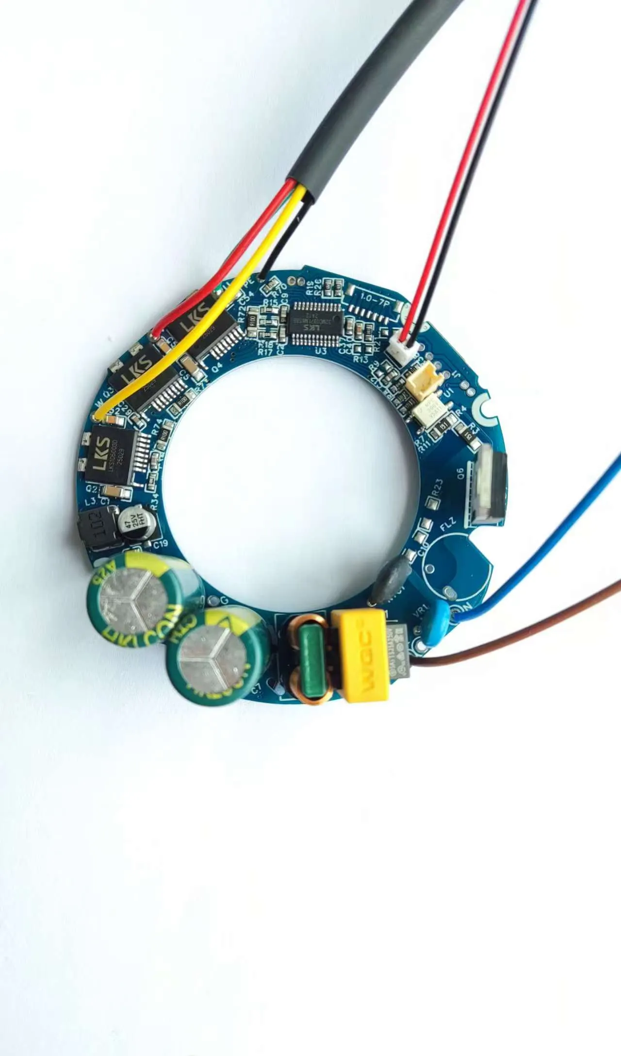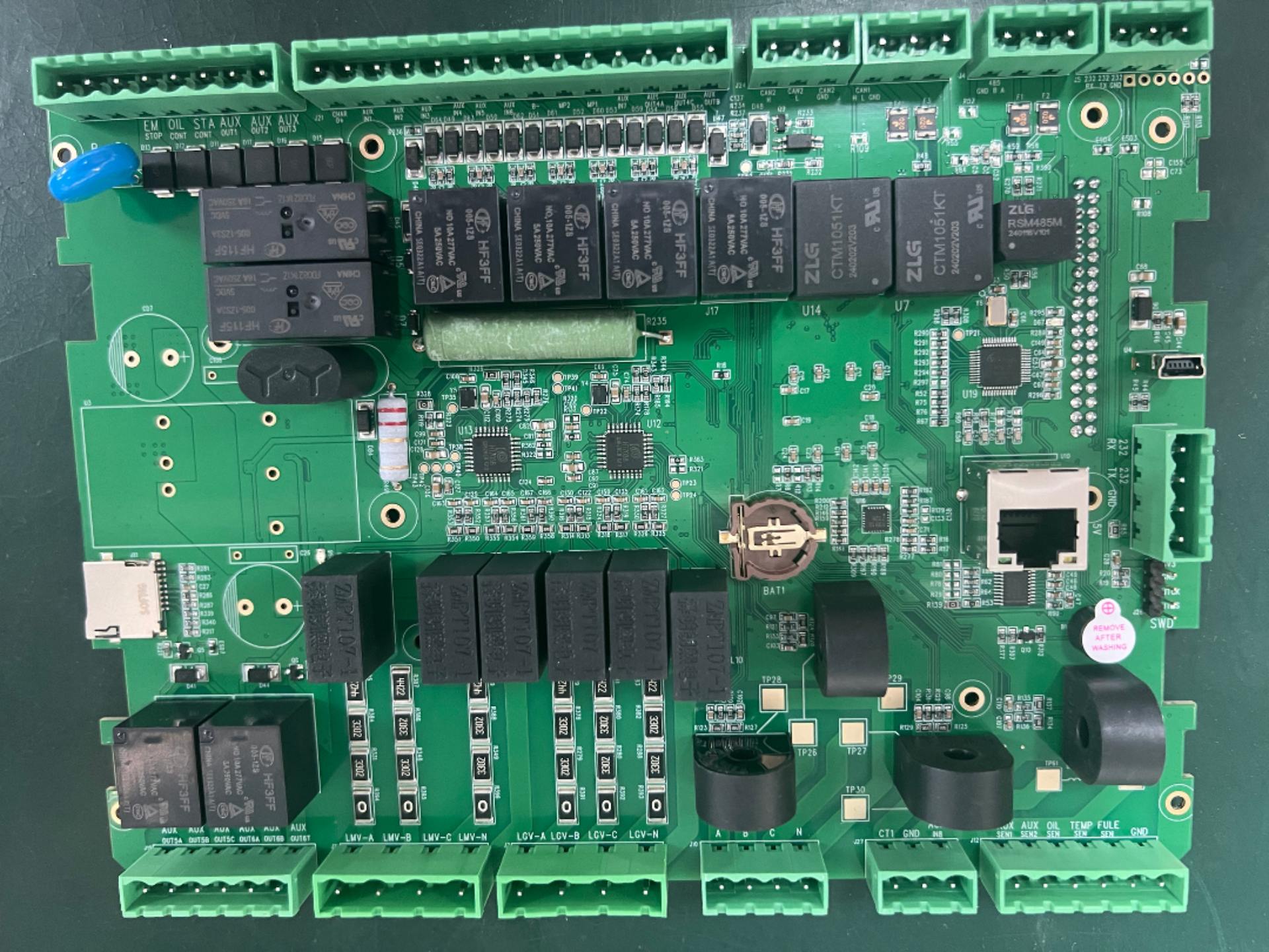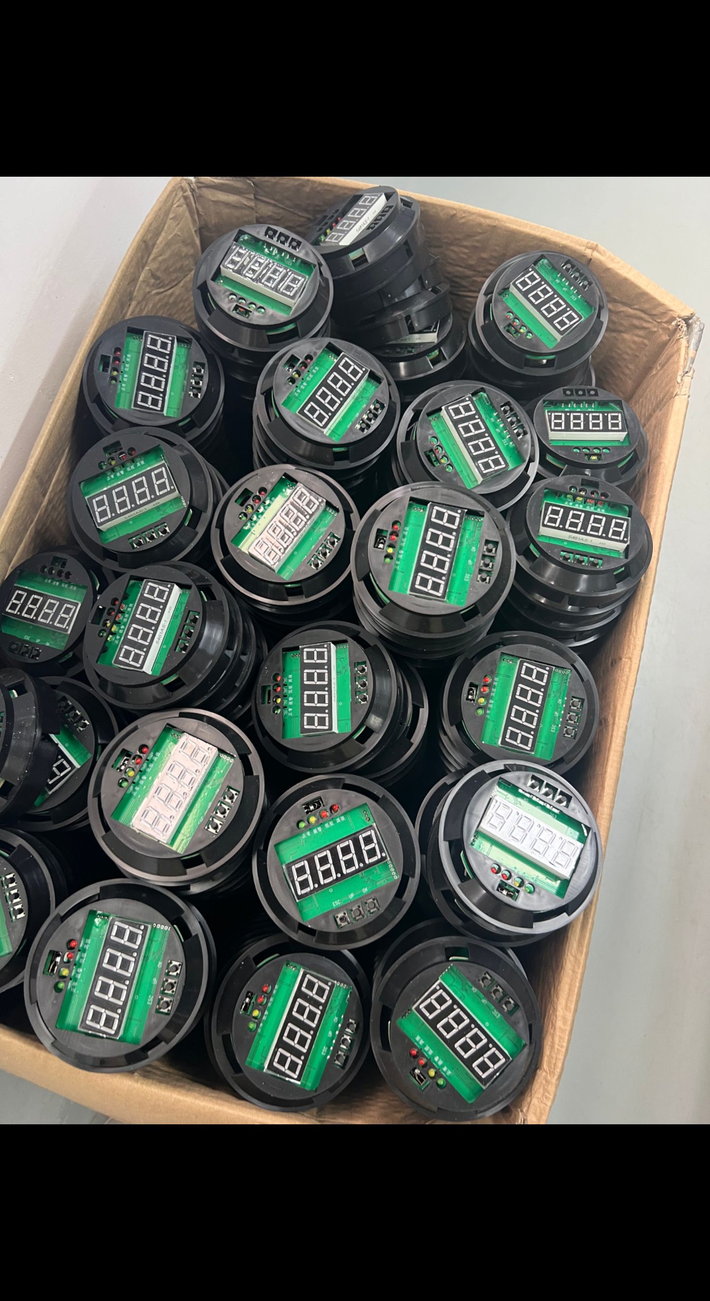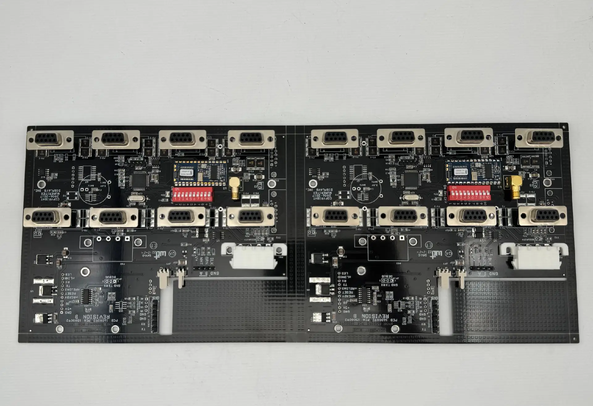
When your design carries 50A, 100A, or more, standard 1oz copper stops being a reliable option.
Thermal stress goes up. Current density becomes a real risk. And not every fab can handle the process cleanly.
We see this most often in power supplies, EV charging modules, industrial motor drives, and solar inverters.
The board is no longer a passive carrier. It’s a thermal and electrical path that has to survive repeated load cycles.
Here’s where thick copper gets difficult:
· Etching precision drops as copper weight increases.
· Plating uniformity becomes harder to control on high-current layers.
· Drilling and through-hole plating must support high aspect ratios without voids.
· Lamination stress rises with unbalanced copper distribution.
That’s why we treat thick copper as a separate process flow, not a normal FR-4 job with extra ounces.
Our typical capability covers 3oz to 10oz finished copper on outer layers.
For mixed designs, we combine thick copper power layers with fine-pitch signal layers in the same stack-up.
That lets you keep control circuitry dense while still handling high current on dedicated layers.
Quality control is built around the failure modes that matter:
· Microsection analysis on every lot to verify copper thickness and plating integrity.
· Thermal stress testing per IPC-TM-650 for high-current boards.
· Impedance modeling adjusted for actual copper profile after plating.
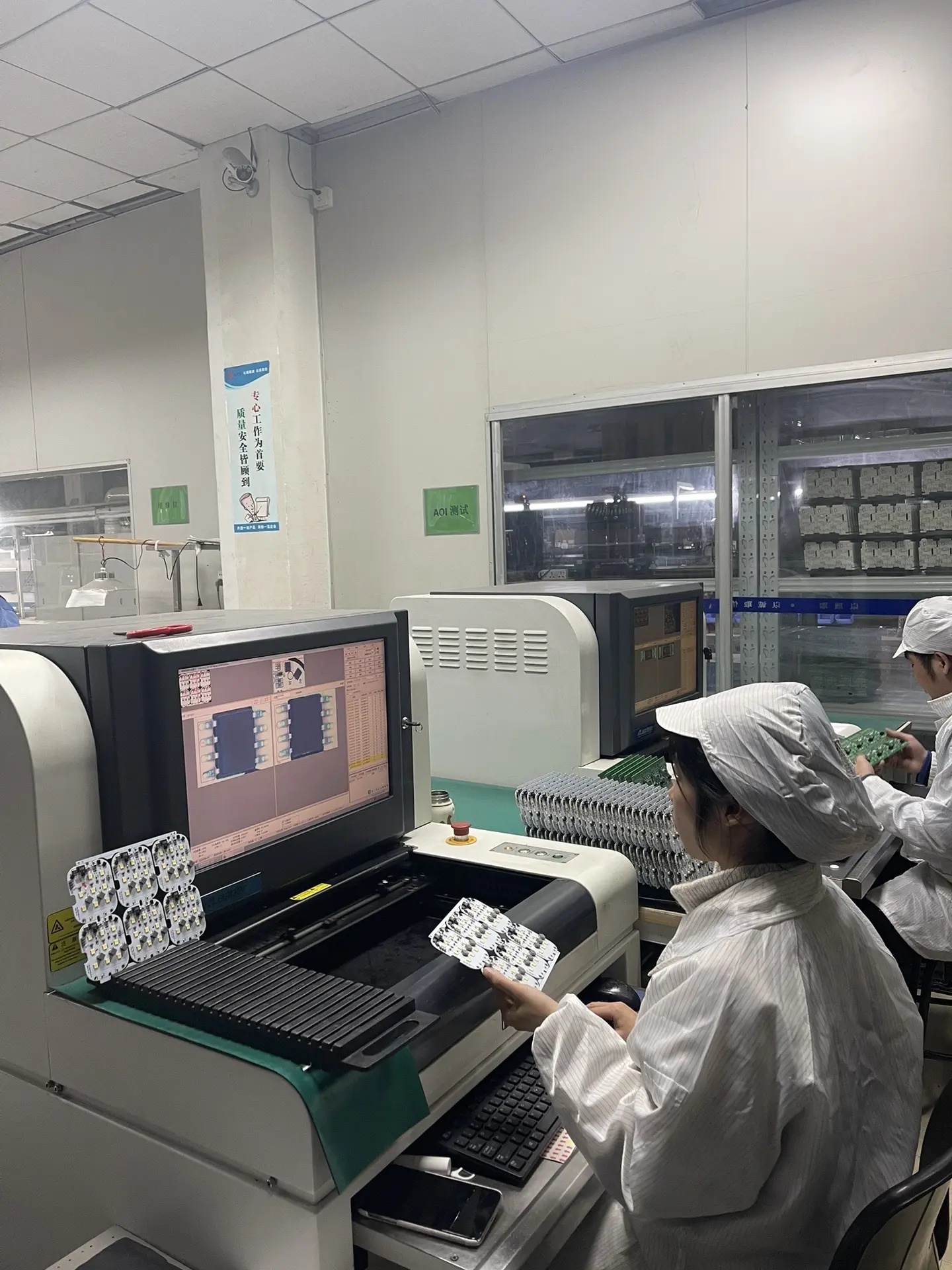
· AOI tuned for thick copper trace definition, not just standard artwork comparison.
This is especially important for quick-turn prototypes.
You don’t want to validate a power design on 1oz or 2oz copper, then find out later the real 6oz version behaves differently under load.
We support thick copper prototypes without forced MOQ.
DFM feedback comes before production, so issues like minimum trace width, spacing, and via structure get resolved early.