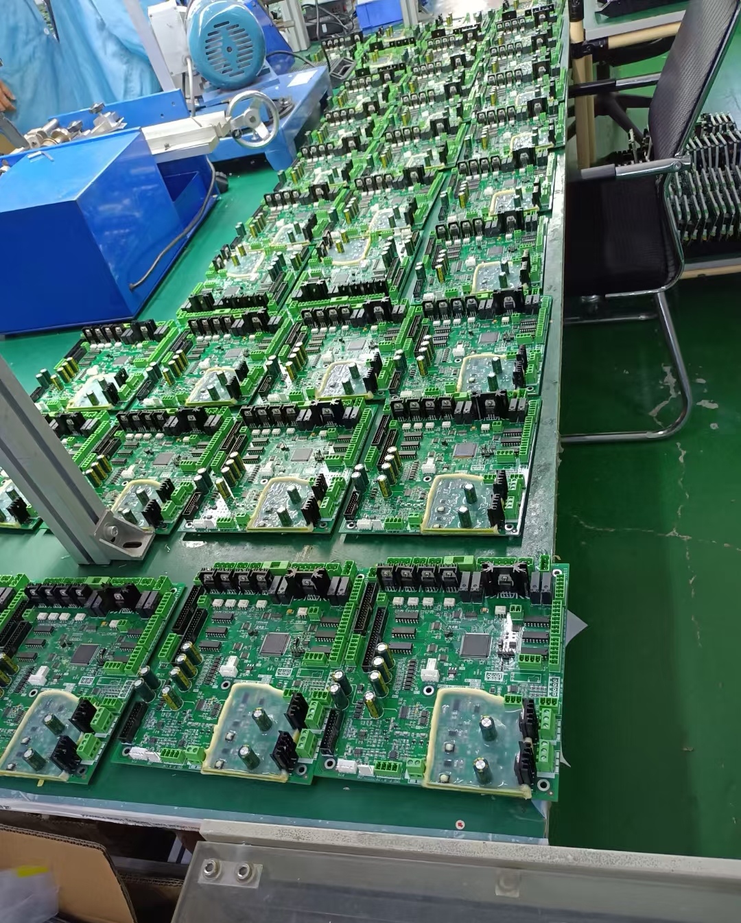
Gold Fingers refer to a row of gold-plated conductive contacts on the edge of PCBs. Physical plug-and-play connection enables signal and power transmission between boards, as well as between boards and equipment. They are widely applied to memory modules, graphics cards, PCIe cards, industrial control boards, vehicle-mounted modules and more.
1. Basic Structure
A gold finger is not simply a layer of gold plating; it adopts a three-layer structure: copper substrate + nickel barrier layer + gold surface layer.
1. Bottom Layer: Copper foil (conductive substrate). Standard 1oz/2oz electrolytic copper serves for electrical conduction. Copper foil will be thickened to reduce resistance for high-current and high-frequency applications.
2. Middle Layer: Nickel plating (critical barrier layer), with a thickness of 3~5μm. It prevents copper atom diffusion, avoids blistering and blackening of the gold layer, and improves overall hardness and wear resistance.
3. Surface Layer: Gold plating (functional layer). Gold features superior conductivity, permanent oxidation resistance and corrosion resistance, ensuring stable low contact resistance for long-term use.
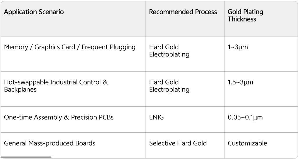
2.1 Hard Gold Electroplating
Composition: Gold-cobalt / gold-nickel alloy, high hardness and excellent wear resistance.
Thickness: 1~3μm (30~100 μin)
Plug lifespan: Over 500~1000 insertions and extractions
Application: Memory sticks, graphics cards, PCIe ports, industrial control cards and frequently plugged interfaces
Features: Relatively high cost; the standard process for gold fingers
2.2 Electroless Nickel Immersion Gold (ENIG)
Advantages: High gold purity, flat surface, great solderability
Thickness: 0.05~0.1μm (ultra-thin)
Disadvantages: Poor wear resistance; copper substrate is easily exposed after repeated plugging
Application: One-time assembly, precision sensors, BGA areas, boards with minimal plugging cycles
2.3 Selective Gold Plating
Gold is only plated locally on gold fingers, while the rest of the PCB receives standard surface treatment. This balances performance and cost, making it the most common mass-production solution.
Process Selection Table by Application Scenario
3. Key Design Specifications
1. Chamfer: The front end of gold fingers is machined into a 30°, 45° or 60° bevel. The bevel guides smooth insertion and prevents scratching contacts and slots during forced plug-in.
2. Key Notch: A small cutout on memory modules. Notches sit at different positions for different memory generations, preventing misalignment insertion and circuit burnout.
3. Staggered Pin Length Design: Power and ground pins are longer than signal pins. On insertion, power connects first followed by signals; on extraction, signals disconnect first then power. This eliminates signal bounce and latch-up effects during plug cycles.
4. Side Protection: Test pads or protective ground traces are usually laid beside gold fingers, supporting factory testing and ESD static protection.
4. Common Failure Modes & Pain Points
2. Gold Layer Abrasion: Repeated plugging wears through the gold layer, exposing nickel or copper underneath. Contact resistance spikes sharply, causing memory blue screens and graphics card display artifacts. High-end server memory is often restricted from frequent plugging for this reason.
3. Peeling & Cracking: Poor PCB base material (low TG value) or defective electroplating leads to gold foil warping under heat or mechanical stress.
5. Maintenance Guidelines
2. Minimize Plug Cycles: Avoid unnecessary insertion and extraction; leave memory sticks plugged once installed.
3. Anti-static Handling: Hold PCBs by the edge frames instead of touching gold finger contacts. Salts and oils from skin accelerate corrosion.
4. Inspection: Use a high-magnification magnifier to check contacts for black spots, indentations or worn-through plating.