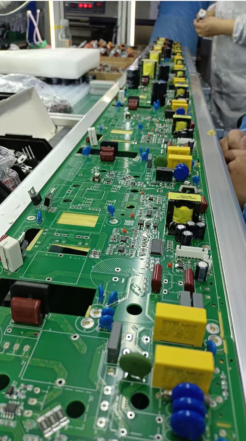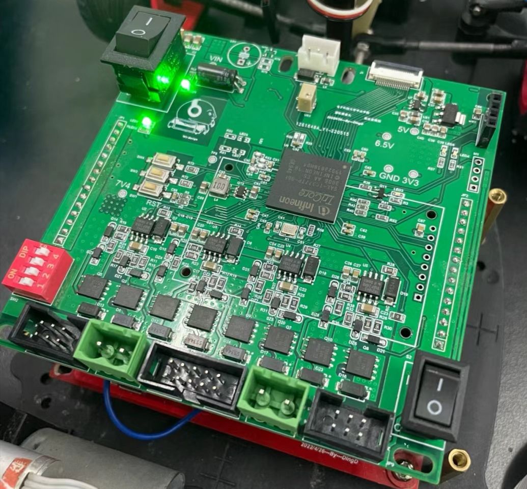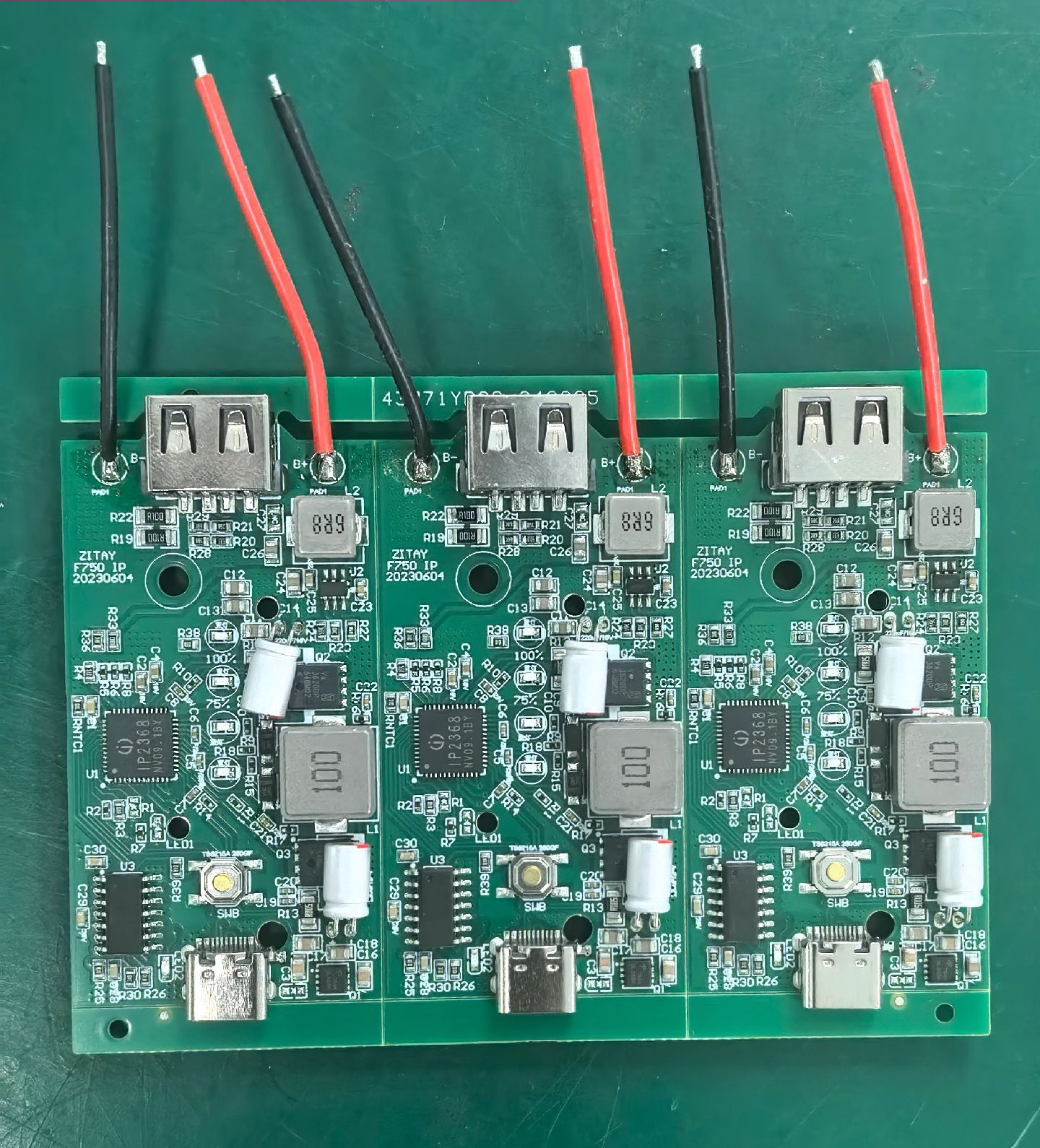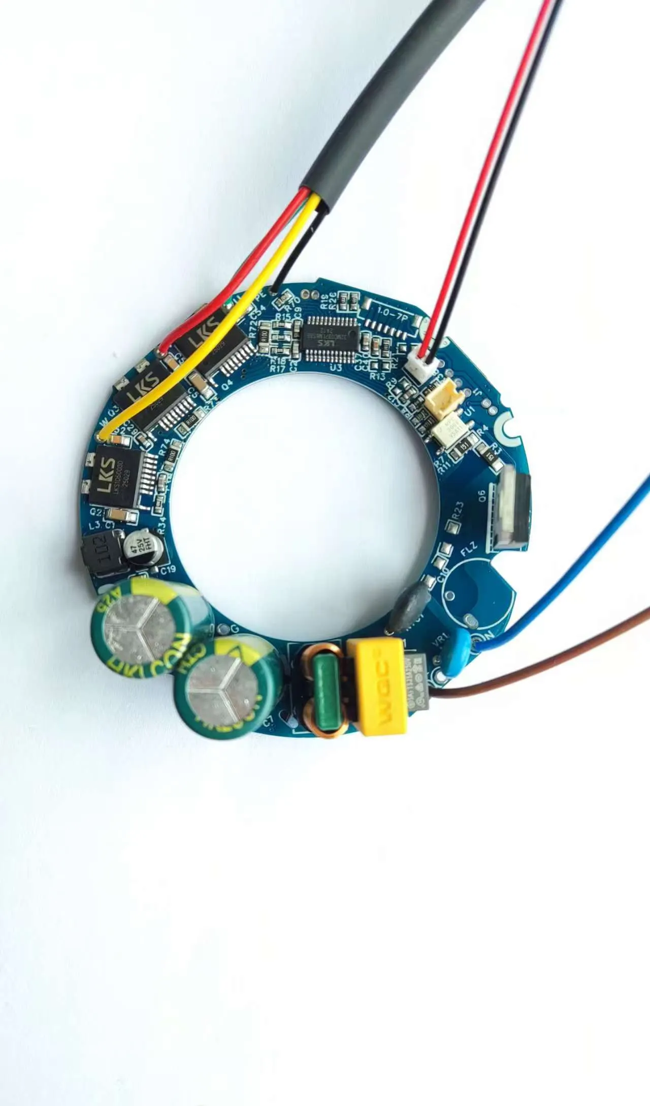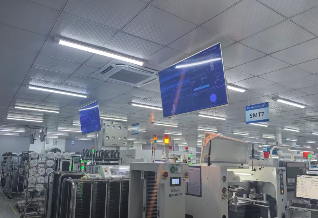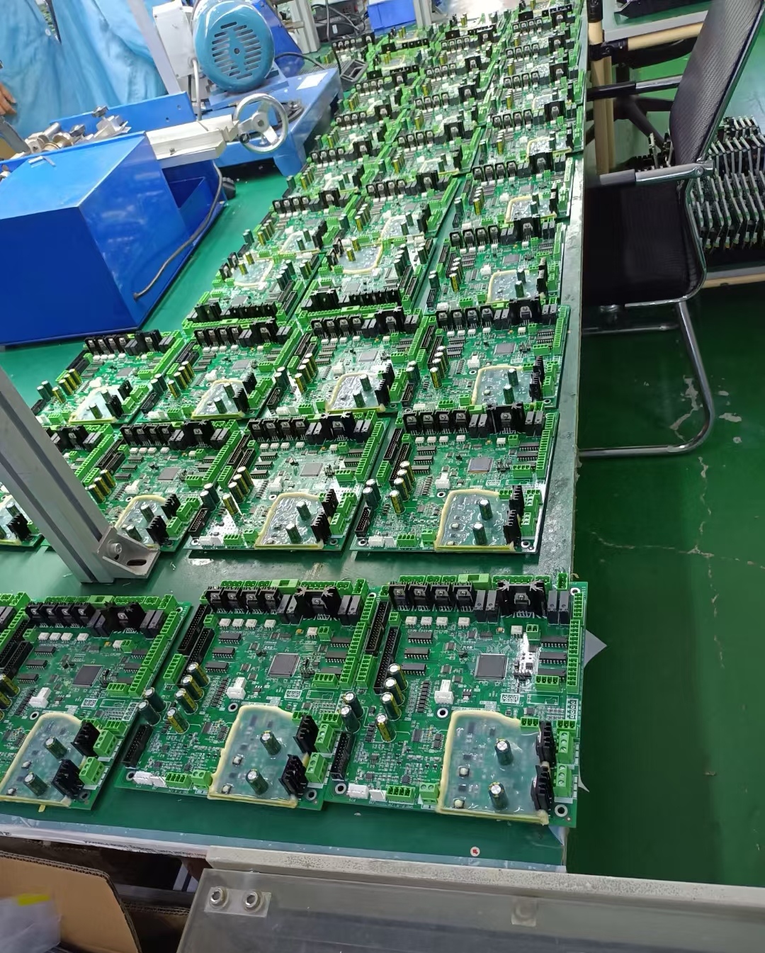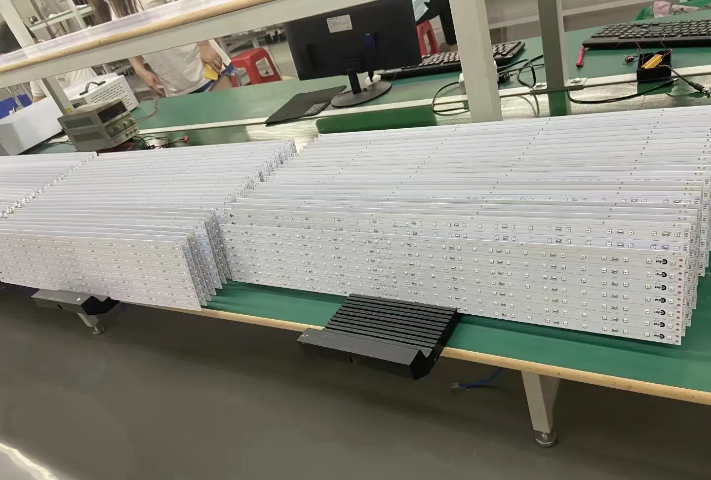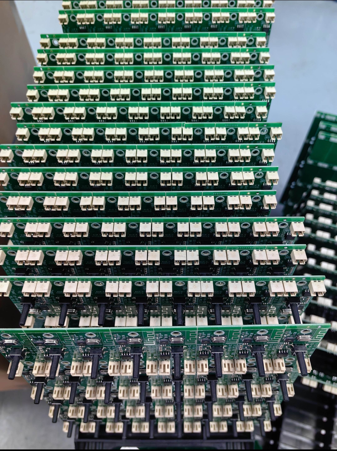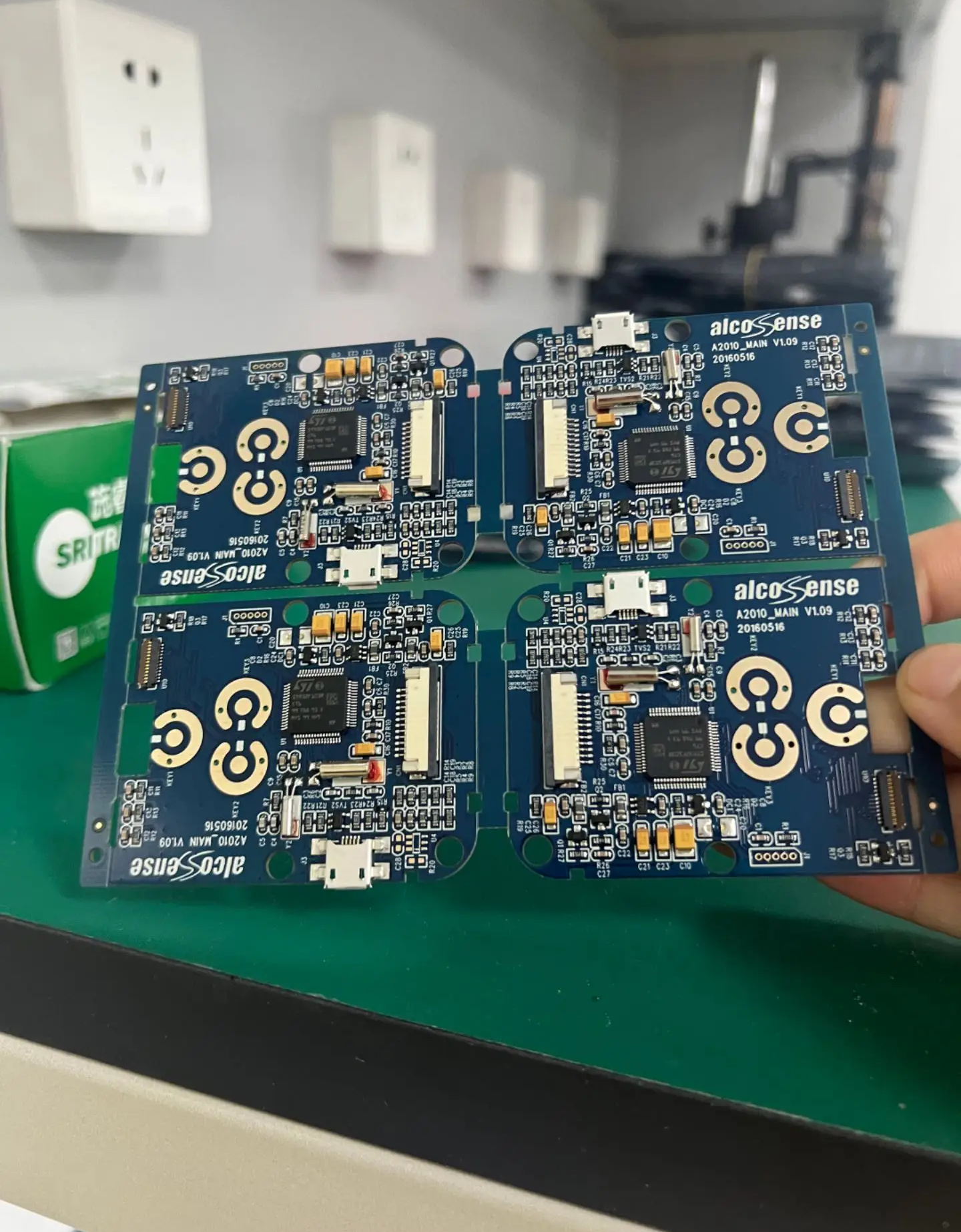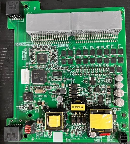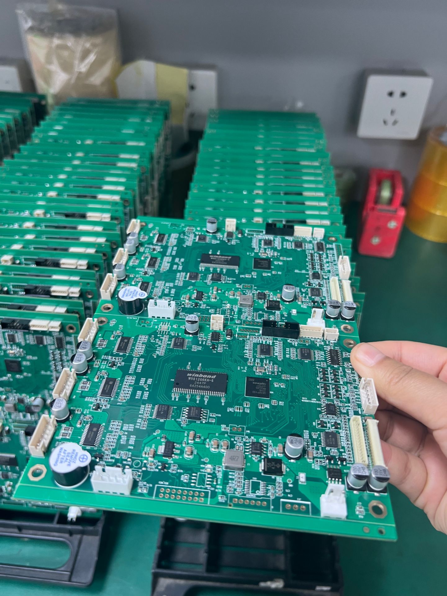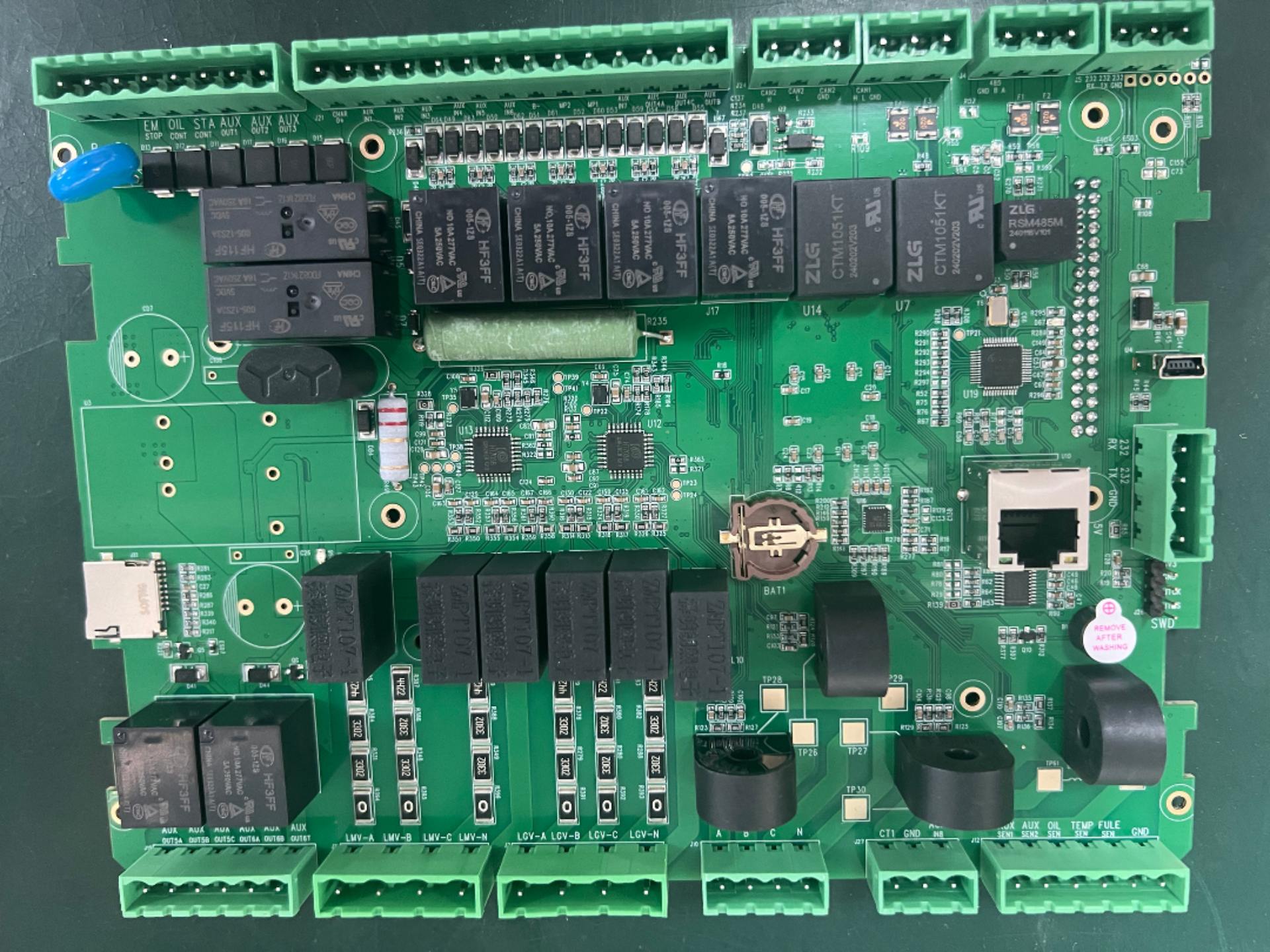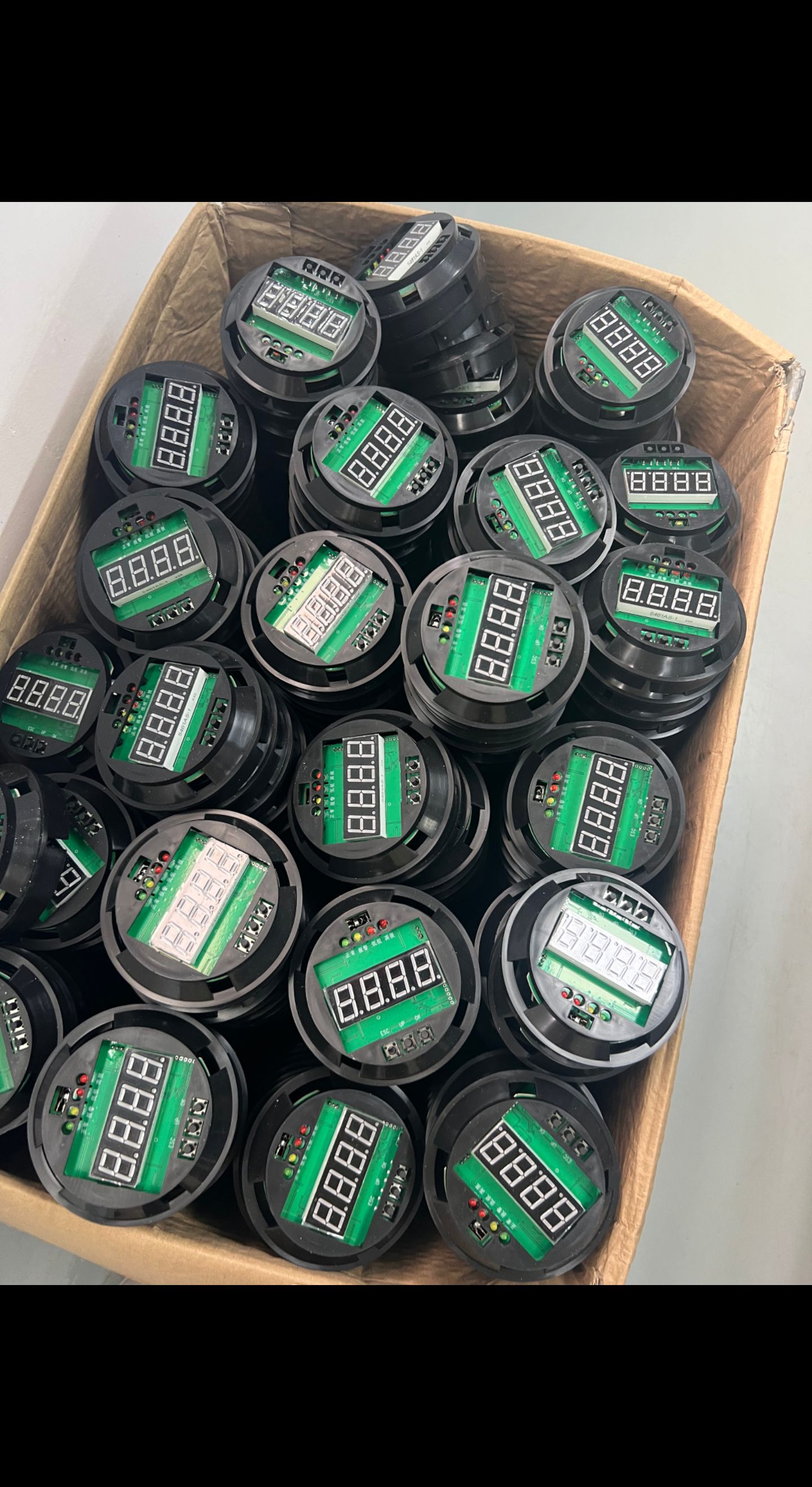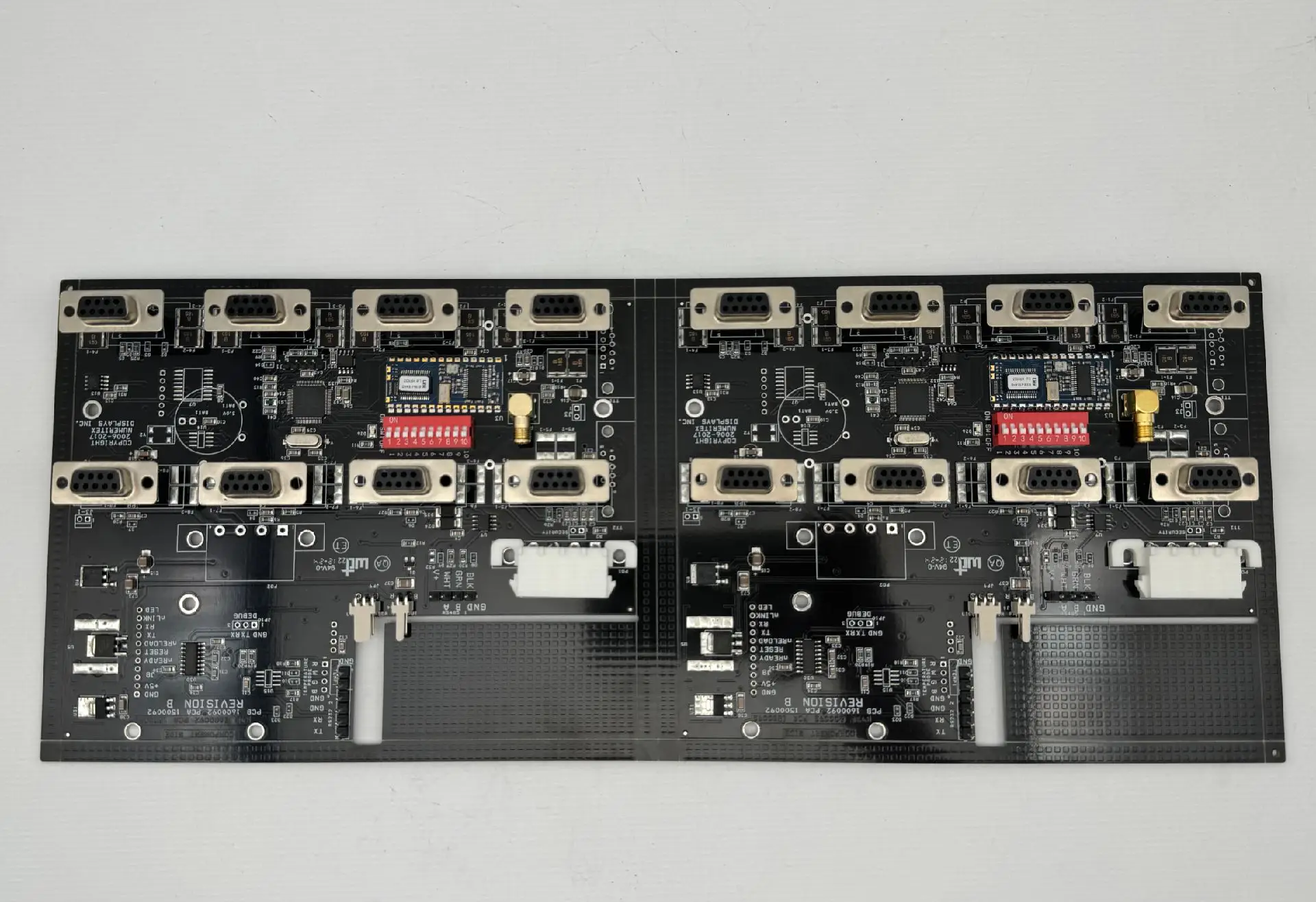
When you pick up your phone, start your car, or operate a medical device, a stably running printed circuit board (PCB) is working silently behind the scenes. As a manufacturing company rooted in the PCB production field, we deeply understand that a fingernail-sized circuit board embodies dozens of precision processes and rigorous quality adherence. Today, let us take you into our production workshop to unveil how a high-quality PCB transforms from a design file into a precision product.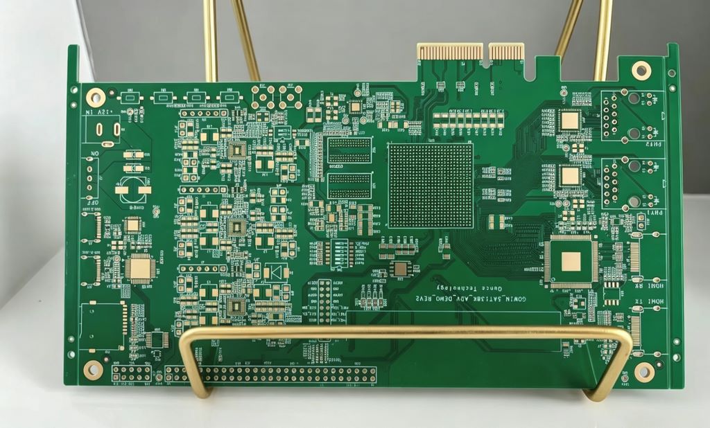
1. From File to Film: Precise Inner Layer Image Transfer
Everything starts with the customer’s design file. After our CAM engineers complete analysis and compensation, a high-precision laser photoplotter draws the circuit patterns onto sheets of optical film. This creates a "negative" for the circuit board, with micron-level accuracy, laying the foundation for subsequent image transfer.
2. Inner Layer Fabrication: Making Copper Foil "Grow" Circuits
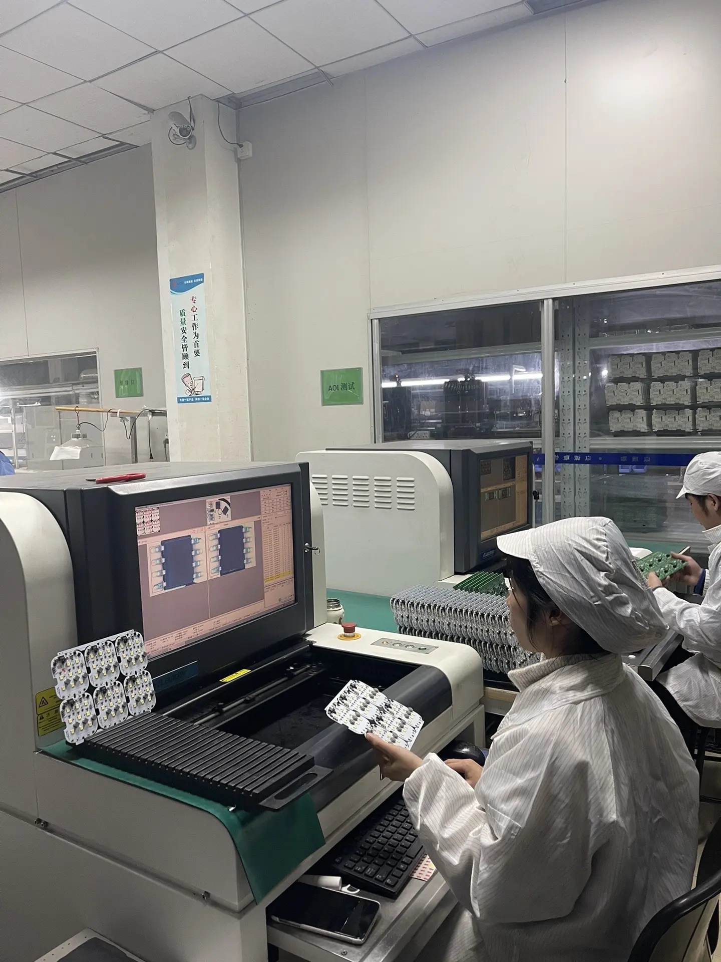
We select high-quality copper-clad laminates. In a cleanroom environment, dry film is tightly laminated onto the copper surface. Ultraviolet light is then used to transfer the film pattern onto the dry film through exposure. After developing, the unexposed areas are washed away, revealing the copper traces that need to be retained. Through acid etching, the unwanted copper foil is completely removed. At this point, the fine inner layer circuit pattern appears on the substrate. Afterward, every inner layer panel undergoes Automated Optical Inspection (AOI), where any tiny open or short circuit is accurately identified and flagged.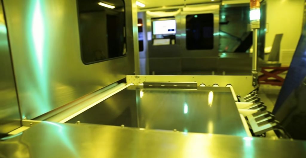
3. Lamination: Bonding Thin Sheets into a Rugged Multilayer Structure
For multilayer boards, multiple fabricated inner layer cores and prepreg sheets are stacked alternately. We use a high-temperature, high-pressure vacuum lamination process, which melts the prepreg and completely fills the gaps between circuit traces, bonding all layers tightly into one. Precisely controlling the heating rate and pressure is key to avoiding delamination and warpage, directly determining the final product’s reliability.
4. Mechanical Drilling and Laser Drilling: Creating Conductive "Tunnels"
On the laminated board, holes must be drilled to achieve interlayer connections. For conventional through-holes, we use high-speed CNC drilling machines to drill tiny holes in the board. For HDI high-density boards, UV or CO₂ lasers drill blind micro-vias as fine as one-tenth the diameter of a human hair. After drilling, the smear inside the holes is thoroughly removed by plasma or chemical processes, ensuring the reliability of subsequent plating.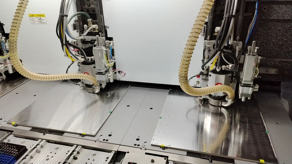
5. Hole Metallization and Pattern Plating: Turning Hole Walls into Conductors
The hole walls of the substrate are inherently non-conductive. Through an electroless copper deposition process, a dense thin layer of copper is deposited on the hole walls, making them conductive pathways. Subsequently, panel plating thickens the copper layer. Then, dry film is applied again, exposed, and developed. Pattern plating further thickens the copper in designated areas, forming robust traces and annular rings. This step determines the current-carrying capacity and is the quality core for power boards and heavy copper boards.
After pattern plating, the dry film is stripped, and the excess copper is etched away. At this moment, the complete circuit pattern is finally revealed. Immediately followed by a second AOI inspection, optical scanning compares against the original design to ensure every trace width and spacing is flawless.
7. Solder Mask, Legend, and Surface Finish: Dressing the PCB in Protective Armor
After the circuitry is completed, we apply green or other colored solder mask ink to the board surface, precisely leaving the pads to be soldered exposed. This protects the traces and prevents solder bridges. Next, component symbols and identifiers are printed via screen printing or inkjet legend printing. Finally, based on requirements, surface finishes are applied to the pads—such as ENIG (Electroless Nickel Immersion Gold), hard gold plating, lead-free HASL, or OSP organic protective film—giving the pads excellent solderability and oxidation resistance.
8. Electrical Test and Final Inspection: No Defective Product Escapes
This is the last checkpoint before shipment. We use flying probe testers or dedicated test fixtures to fully inspect every single board, ensuring all nets are connected, insulation is normal, and there are no opens or shorts. Meanwhile, impedance testing, thermal stress testing, solderability testing, and even cross-section analysis are conducted according to the board’s classification. Only boards that pass all tests are allowed to be packaged and shipped.
A seemingly ordinary PCB actually goes through eight core steps—image transfer, lamination, drilling, plating, etching, solder mask, and testing—each requiring meticulous precision. In our factory, this process is integrated with high-precision equipment and the rigorous oversight of skilled technicians.