
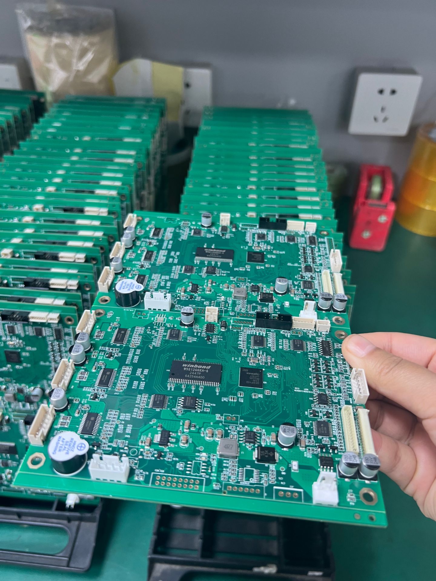
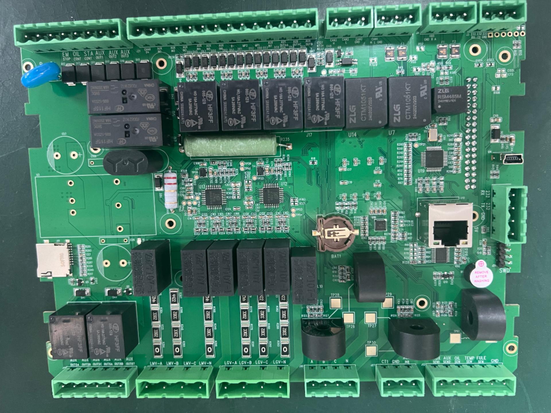
Inside a multilayer PCB, there may be thousands of traces finer than a human hair. A single microscopic open or short, invisible to the naked eye, can render the entire board useless. How do we ensure every board delivered to you is flawless? The answer lies in this critical step – AOI, Automated Optical Inspection.
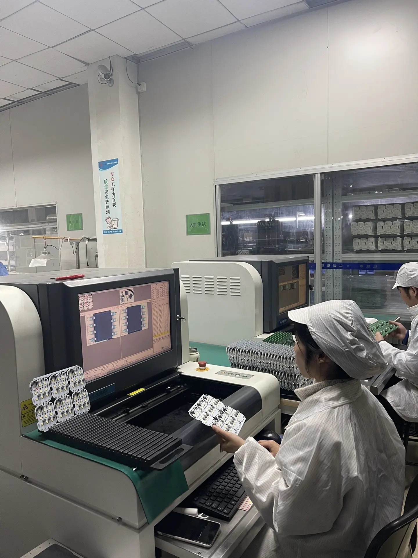
AOI is a non-negotiable quality gate in PCB fabrication. It is deployed after etching on every layer, performing 100% inspection of all circuit patterns. Using high-speed line-scan cameras and multi-angle lighting, the system scans the entire panel with micron-level precision and compares the live image point by point against the original CAM design. Opens, shorts, line width deviations, pinholes, copper slivers, or residual copper – any defect exceeding the acceptance criteria is instantly captured and marked. The true value of this process is simple: it stops defects before lamination, preventing any hidden flaw from being buried inside the layers you cannot see.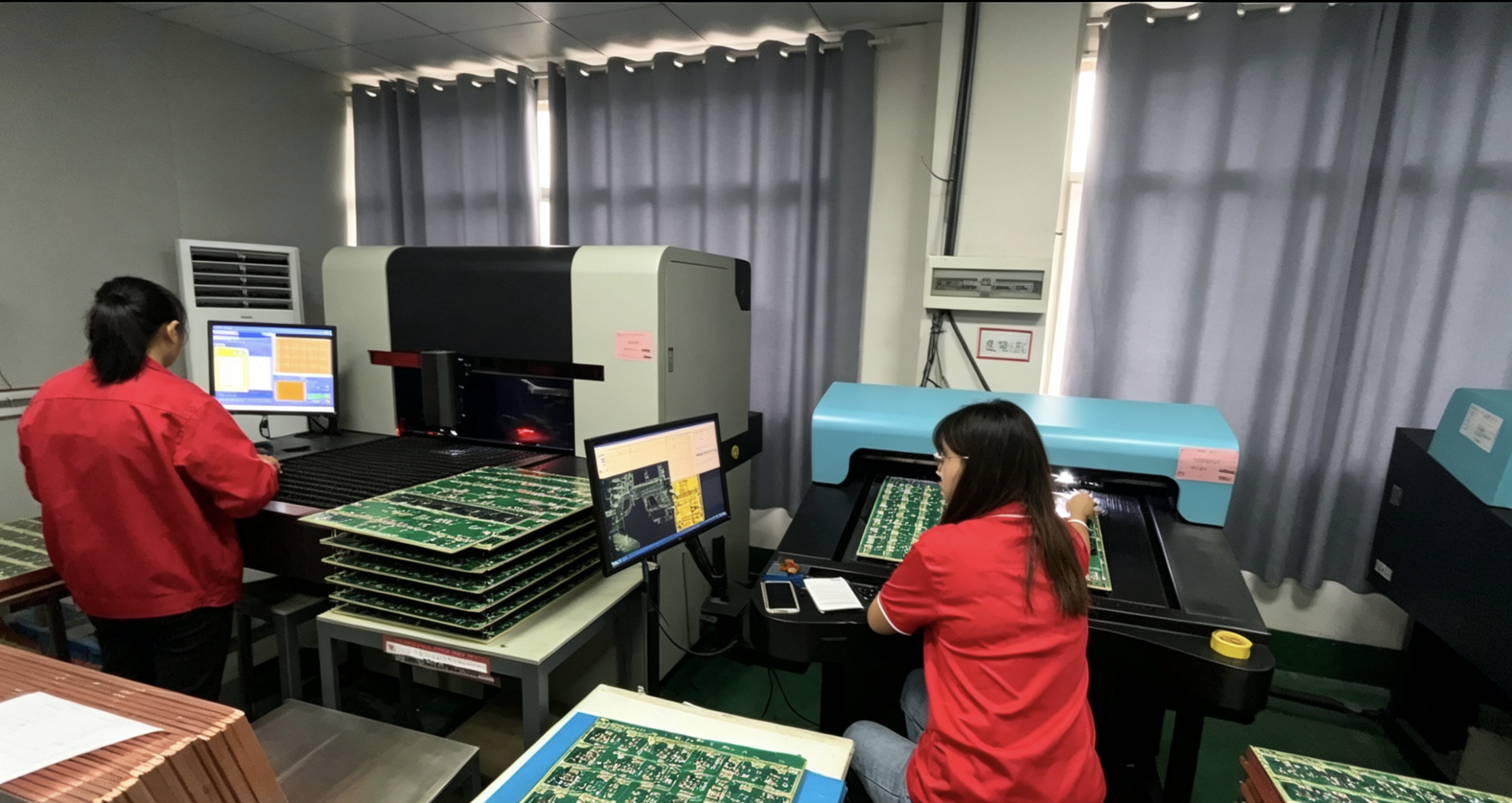
Inner layer AOI is especially critical in multilayer production. Once an inner layer defect is sealed inside by lamination, it becomes completely unrepairable. It may only surface during final electrical test – by which time the entire board is already scrap. AOI blocks these irreversible risks right at the source. Every detected defect is archived, automatically marked, and then manually reviewed by a specialist, who decides whether to repair or reject the board, ensuring only absolutely qualified layers move downstream. At the same time, the process data generated by AOI is fed back in real time to upstream processes, driving continuous optimization of exposure and etching parameters, and reducing defect rates at the root.
Today‘s AOI technology has entered an intelligent era. 3D imaging accurately measures trace height and copper thickness, elevating inspection from 2D to a true volumetric perspective. Deep learning algorithms give the system independent judgment, precisely distinguishing real defects from “false calls” caused by base material texture, driving both escapes and false alarms to an absolute minimum. This is more than inspection – it is a data-driven quality prevention system.
Every PCB delivered to you has passed this “pixel-level” quality trial. AOI uses light as its ruler and algorithms as its eyes, fulfilling a zero-defect promise through 100% inspection, making quality begin between the invisible microns.
10585 View