“A powerful chip is just a ‘naked core’ without it,” a senior packaging engineer once said of the substrate’s importance. Within a space the size of a fingernail, it carries the grand vision of the computing world.
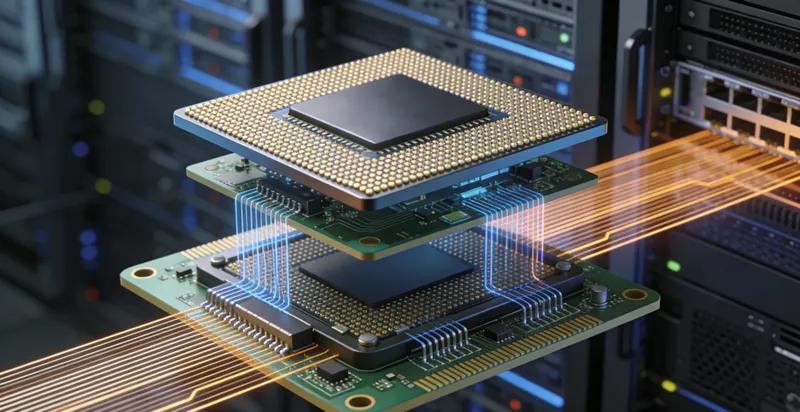
If a regular PCB is the urban road network, an IC substrate is the “neural highway” leading straight to the chip’s core. The global IC substrate market size reached $17.4 billion in 2022 and has continued to grow. What is the evolution of this technological high ground? And what little-known manufacturing secrets does it hold?
01 Technological Evolution: A Century-long Journey from Connecting Wires to the "Chip Foundation"
To understand substrates, we must place them in the entire development history of PCB technology. The emergence of PCBs was a revolution in itself—they replaced the messy physical wire connections in early electronic devices with etched copper lines.
The technological evolution is clear: from single-layer and double-layer boards to multi-layer boards, density and complexity have continued to rise. The real watershed came in the 1980s and 1990s. As semiconductor components became increasingly miniaturized, traditional packaging methods such as lead frames could no longer meet the demands of high-density interconnection.
At this time, Ball Grid Array (BGA) packaging technology emerged. It replaced traditional metal lead pins with an array of solder balls, greatly increasing I/O density. The dedicated circuit board serving this new packaging technology—the IC substrate—was born.
Its role underwent a fundamental shift: no longer merely a platform for supporting and connecting ordinary components, it became an indispensable intermediate carrier between the chip and the motherboard, responsible for transmitting electrical signals, dissipating heat, and providing mechanical protection. Put simply, high-performance modern chip packaging is impossible without high-level substrates.
02 Core Definition: What is a Substrate? Beyond IC Packaging
In a broad sense, a "substrate" is a functional general term referring to a planar medium made of glass, metal, plastic, or other materials, used to support electronic components or fix load phases.
However, in the high-end electronic manufacturing field we discuss, it specifically refers to the IC substrate—the substrate used for integrated circuit packaging. It is a key material in the packaging process, accounting for 70% to 80% of the total cost in high-end packaging.
Together with the familiar rigid and flexible boards, it forms the three major categories of PCBs. If a rigid board is the reinforced concrete main structure of a building, and a flexible board is the flexible connecting pipelines, an IC substrate is a dedicated mounting base for the core components of precision equipment, with the highest technical requirements.
03 Material Division: ABF and BT, the Two Main Technical Routes
The substrate industry is dominated by two major material systems with distinct characteristics and application fields, namely BT substrates and ABF substrates.
BT substrates are based on bismaleimide triazine resin as the core substrate, featuring dimensional stability, high hardness and excellent heat resistance. They are widely used with a market share of over 70%, mainly applied in memory, MEMS sensors, mobile phone RF modules and other products.
ABF substrates use Ajinomoto Build-up Film as the core substrate, with the core advantages of ultra-fine line formation, high pin count and outstanding high-frequency performance. Relying on this feature, it has almost a monopoly on the high-end substrate market, with a market share of over 90% just in the FC-BGA substrate field, and is mainly used in high-performance computing chips such as CPUs, GPUs, FPGAs and high-end server chips.
Due to the technological monopoly of ABF materials, the global substrate supply chain is highly concentrated, with enterprises in Japan, South Korea and Taiwan China accounting for more than 90% of the output value.
04 Manufacturing Core: Build-up Process and the Micron-level Battle
Substrate manufacturing can be called a "micro-engraving art" in the PCB field. Its core process is the build-up method: on the basis of a core board, high-density circuits are constructed by stacking layers one by one through coating insulating media such as polyimide and ABF film, making microvias to realize interlayer connection.
The mainstream processes include Semi-Additive Process (SAP), modified Semi-Additive Process (mSAP) and Electroplating Through Substrate (ETS), which are not detailed in this article and interested readers can refer to relevant materials on their own. The entire manufacturing process requires micron-level precision with strict requirements on core indicators. In terms of line/space, advanced technologies have now achieved 5/5 microns, and the future will challenge 3/3 microns. In the microvia production link, precision technologies such as laser drilling are required to ensure the stability of interlayer connection. In material processing, substrates such as ABF film need to go through a series of complex processes including lamination, laser drilling, desmearing, fine circuit pattern transfer and electroplating.
A tiny deviation in any step may cause signal transmission failures or product reliability loss. Therefore, substrate manufacturing integrates the most cutting-edge equipment and process technologies in the PCB industry, with extremely high capital and technical barriers.
05 Future Battlefield: The High-frequency and High-speed Race Driven by AI
Currently, the high-performance computing demands brought by artificial intelligence and 5G technologies have become the biggest driving force for the development of substrate technology. The explosive growth of chip computing power has put more stringent performance requirements on substrates.
First is lower transmission loss: to adapt to high-speed signal transmission, the dielectric loss factor of insulating materials is required to decrease continuously, with a target of 0.002 or even lower. Second is higher dimensional stability: the substantial increase in chip power consumption leads to more significant thermal expansion and contraction effects, requiring substrates to have a lower coefficient of thermal expansion to ensure the long-term working reliability of equipment. At the same time, there is also a demand for higher integration: to further reduce the packaging volume, more advanced structures such as coreless substrates are under research and development.
This technological competition in the substrate field is not only a contest of manufacturing processes but also a breakthrough in core materials. Breaking the monopoly of ABF materials and developing a new generation of build-up materials with lower dielectric constant and smaller transmission loss has become the core competition direction of the substrate industry chain.
From the first copper-clad laminate in a radio to today’s ABF substrates carrying hundreds of billions of transistors, the development history of PCB technology is a microcosm of electronic products advancing toward smaller, faster and more powerful iterations. When we marvel at the smooth operation of mobile phones and the rapid iteration of artificial intelligence models, we should not forget that beneath the chip, the tiny and complex world of substrates is silently carrying everything.