
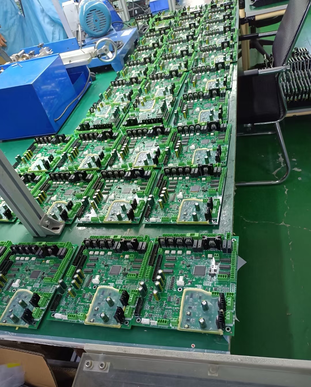
First, select the substrate, cut it to the appropriate size and clean it thoroughly. Then, confirm the production plan, issue materials, and perform cutting. After cutting, lamination is carried out, where multiple layers of substrates are bonded and fixed together under high temperature and pressure. Once lamination is completed, drilling is done, followed by copper deposition and pattern plating. After plating, chemical etchant is used to remove the excess parts, leaving clear circuits.
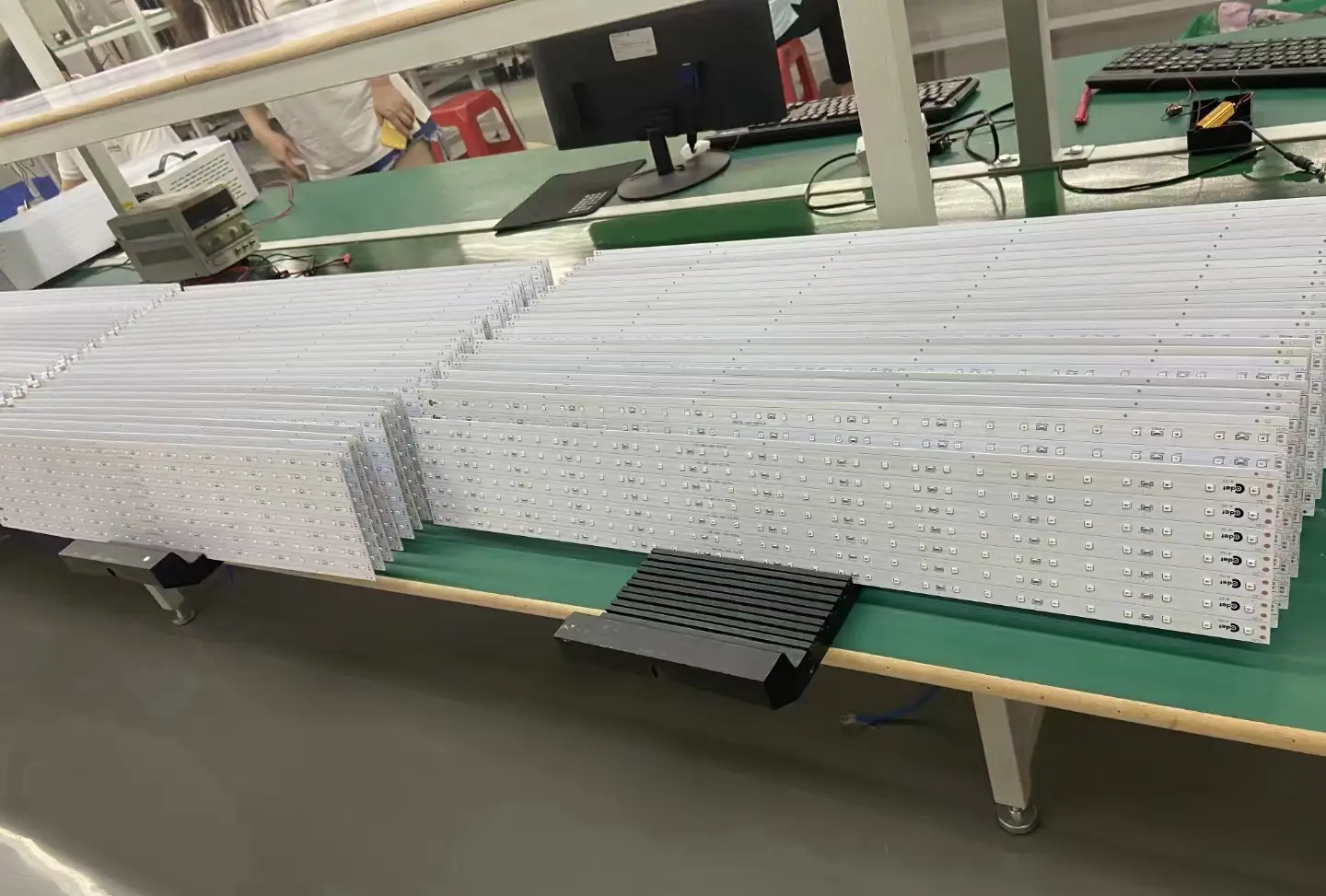
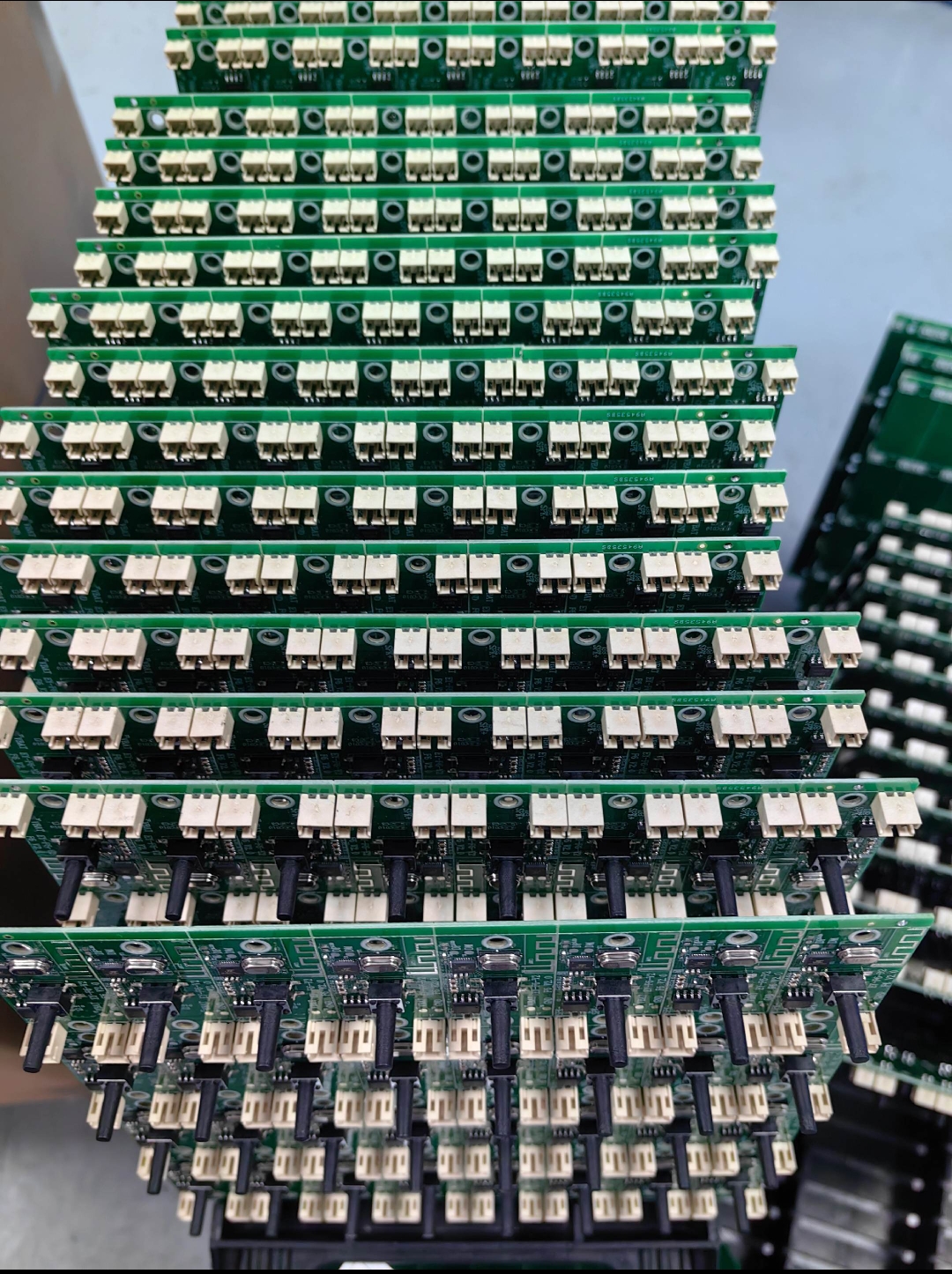
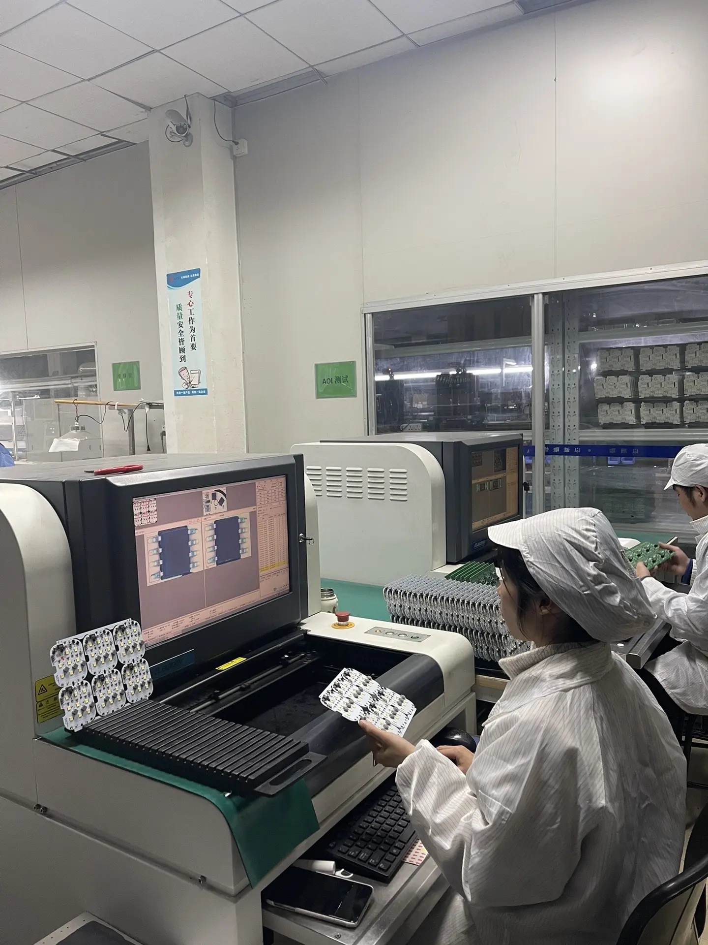
Next, a solder mask is applied, and then the surface is treated to enhance solderability. The process then moves to the shaping stage—using CNC milling, stamping, or other methods to cut the PCB into the final shape specified in the design, removing excess borders and waste materials to meet the installation size standards. After shaping, testing is conducted, and qualified products are packaged.
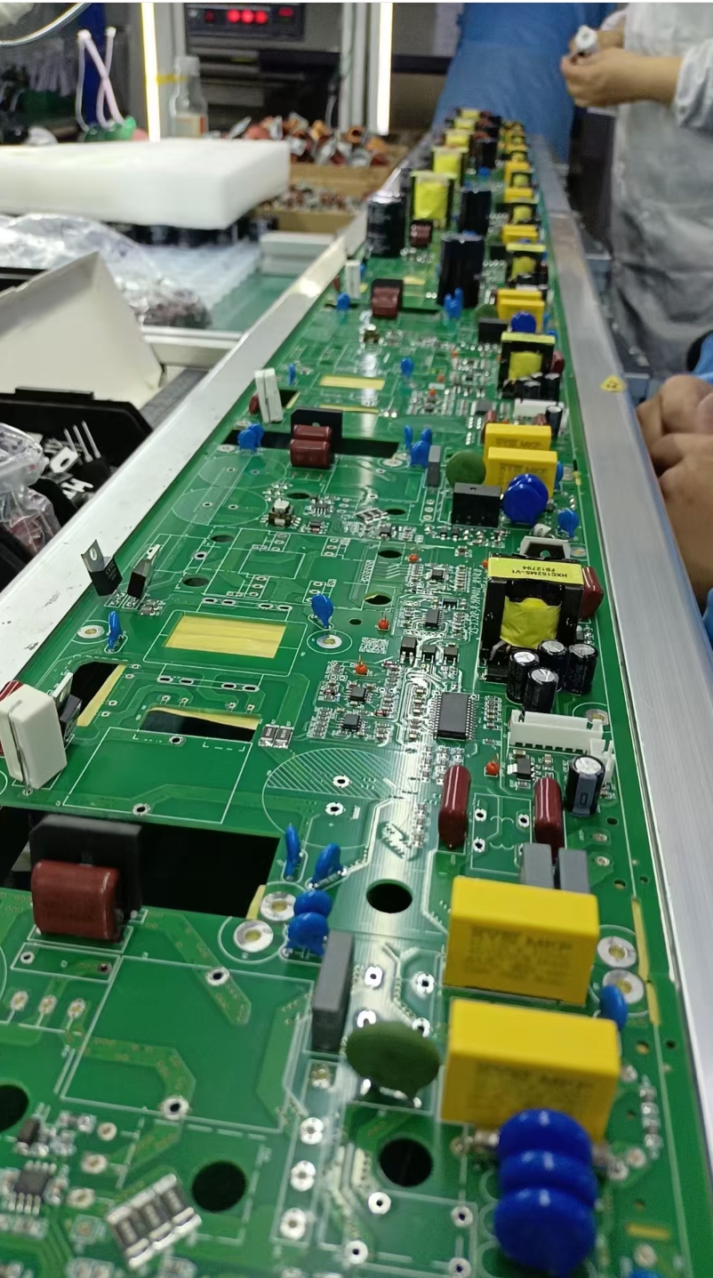
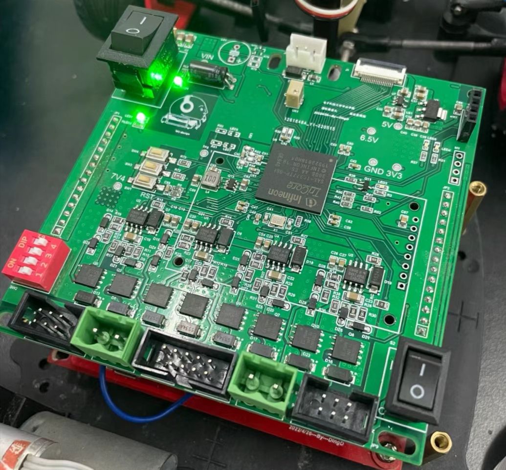
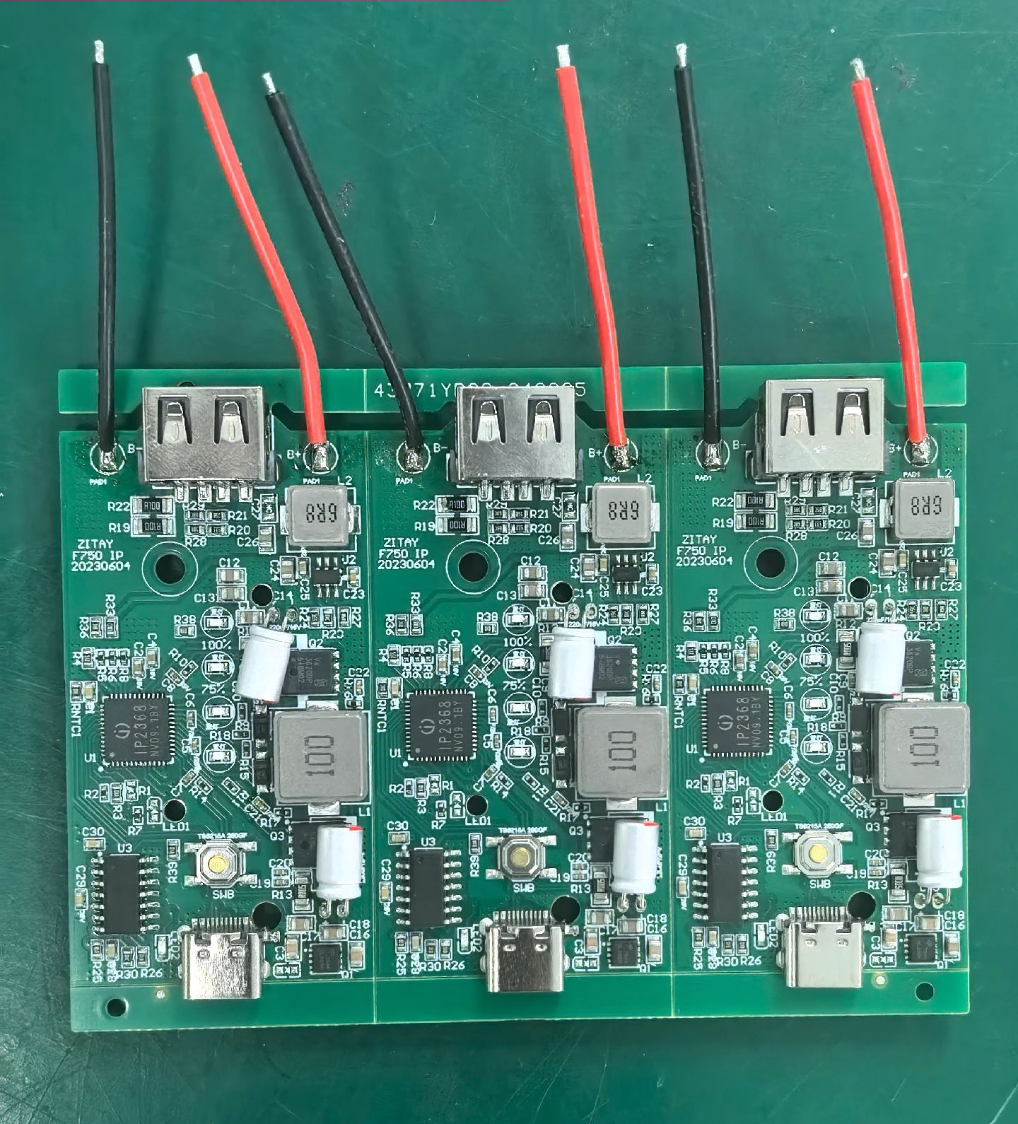
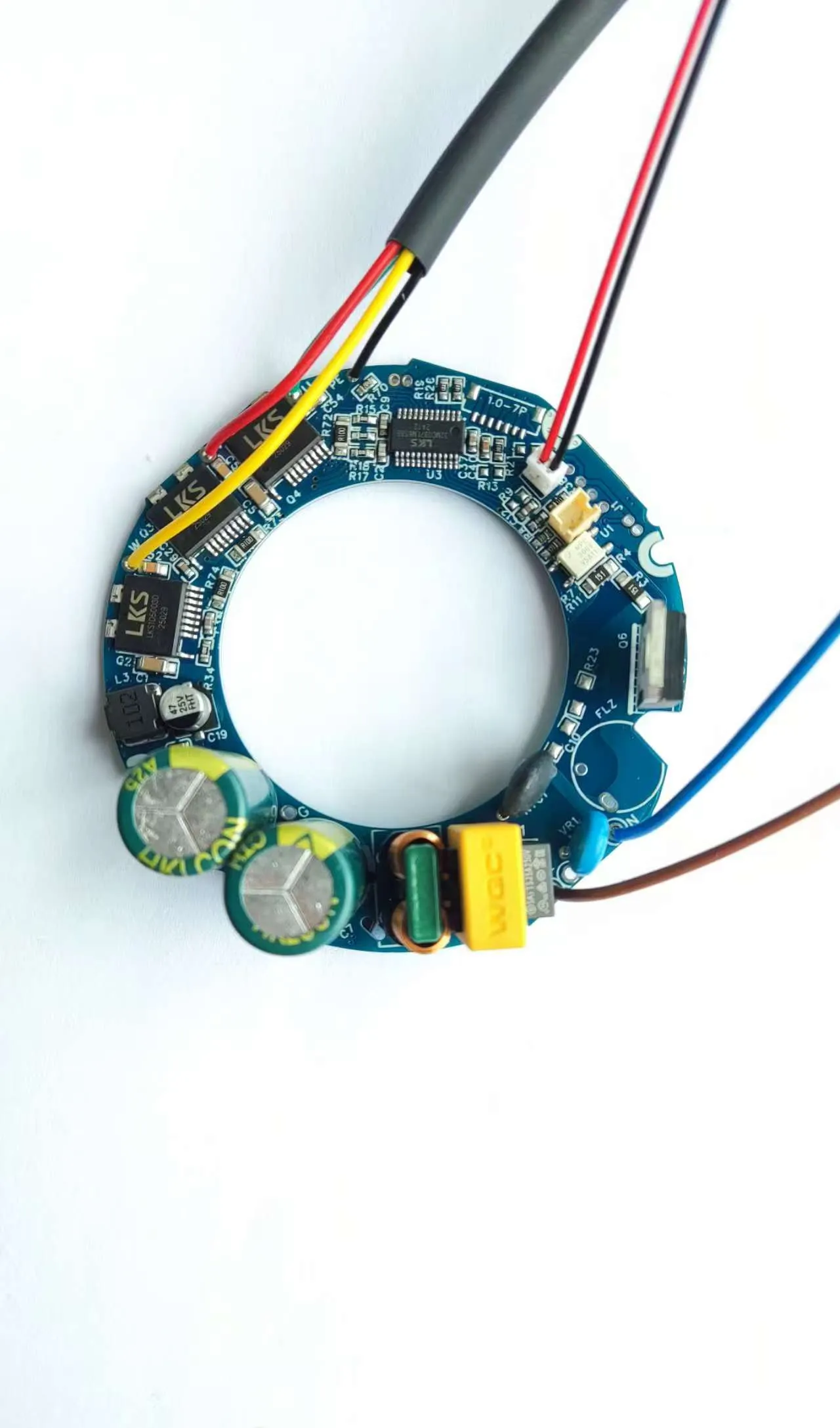
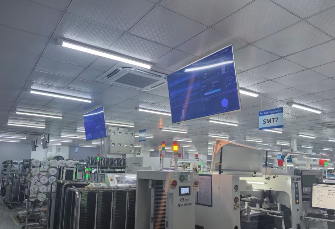
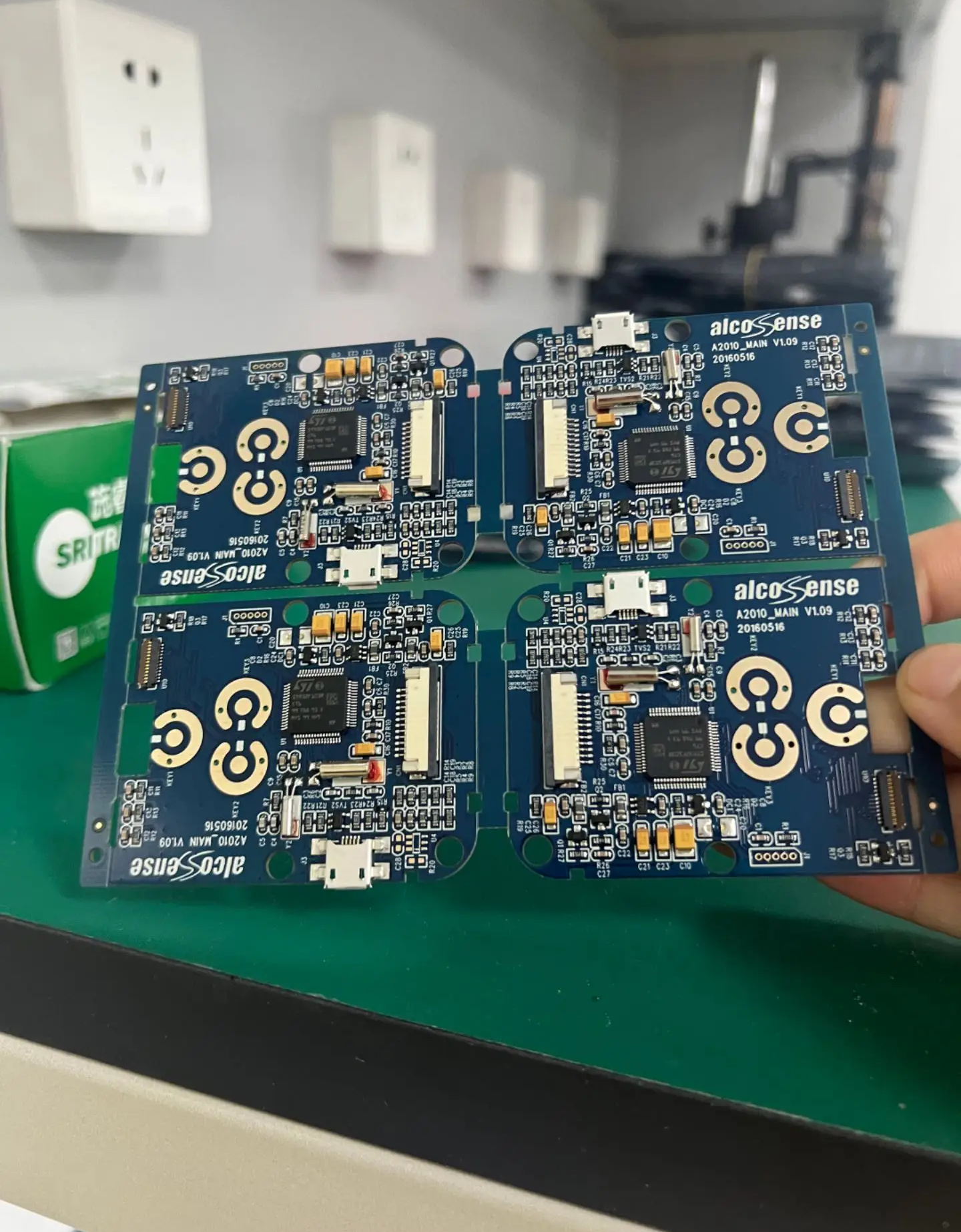
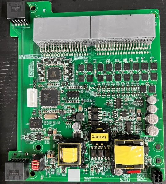
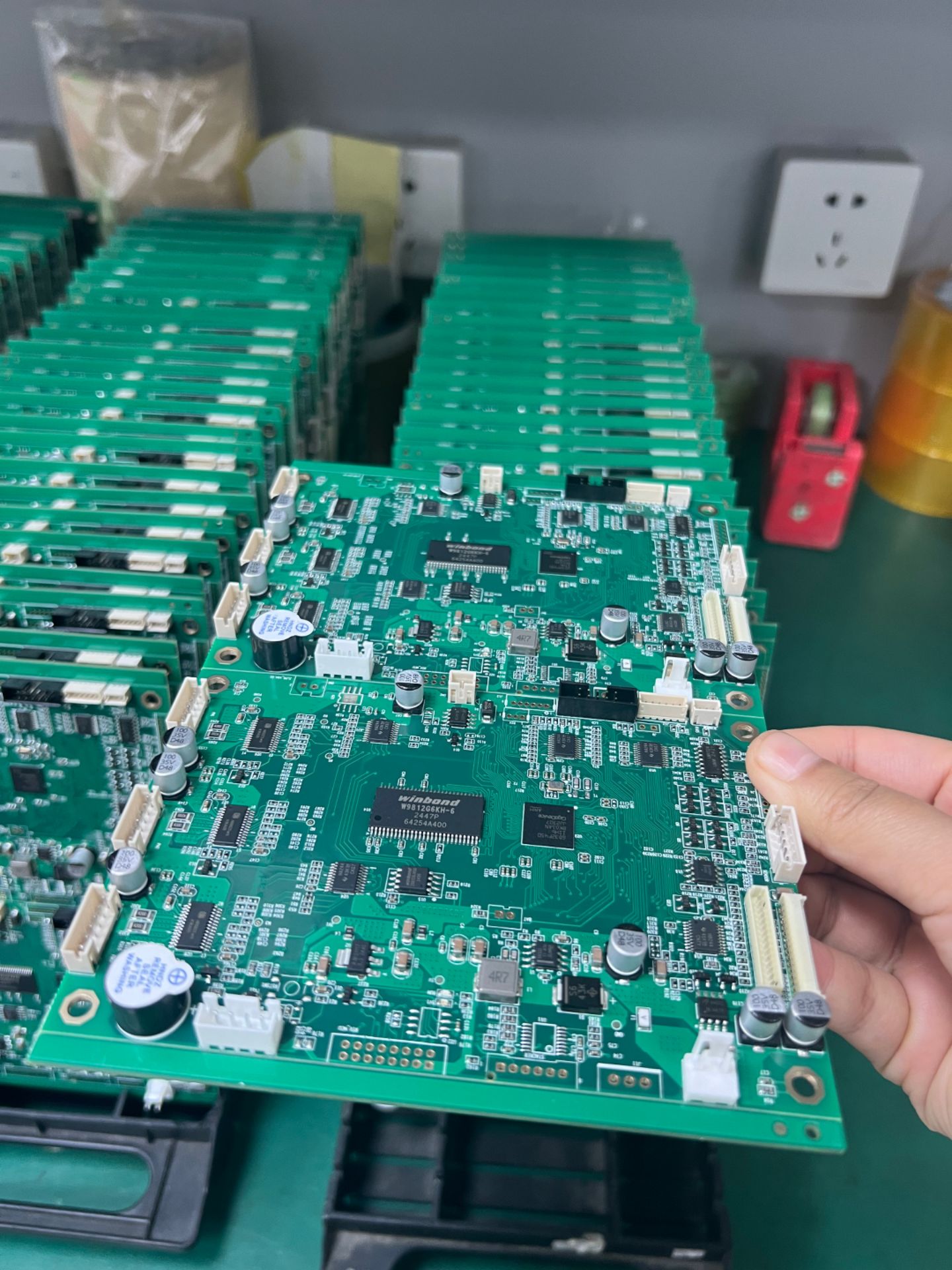
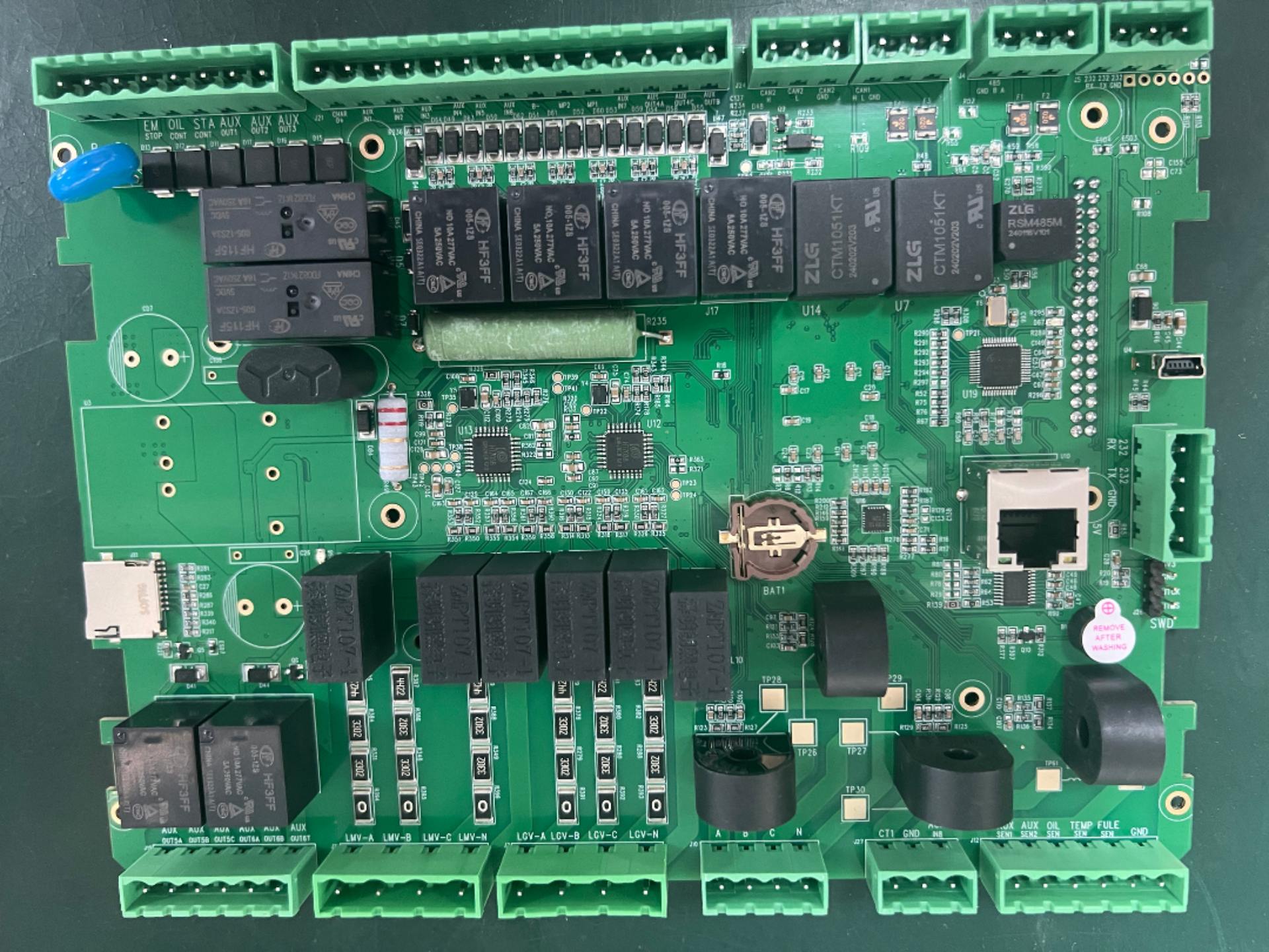
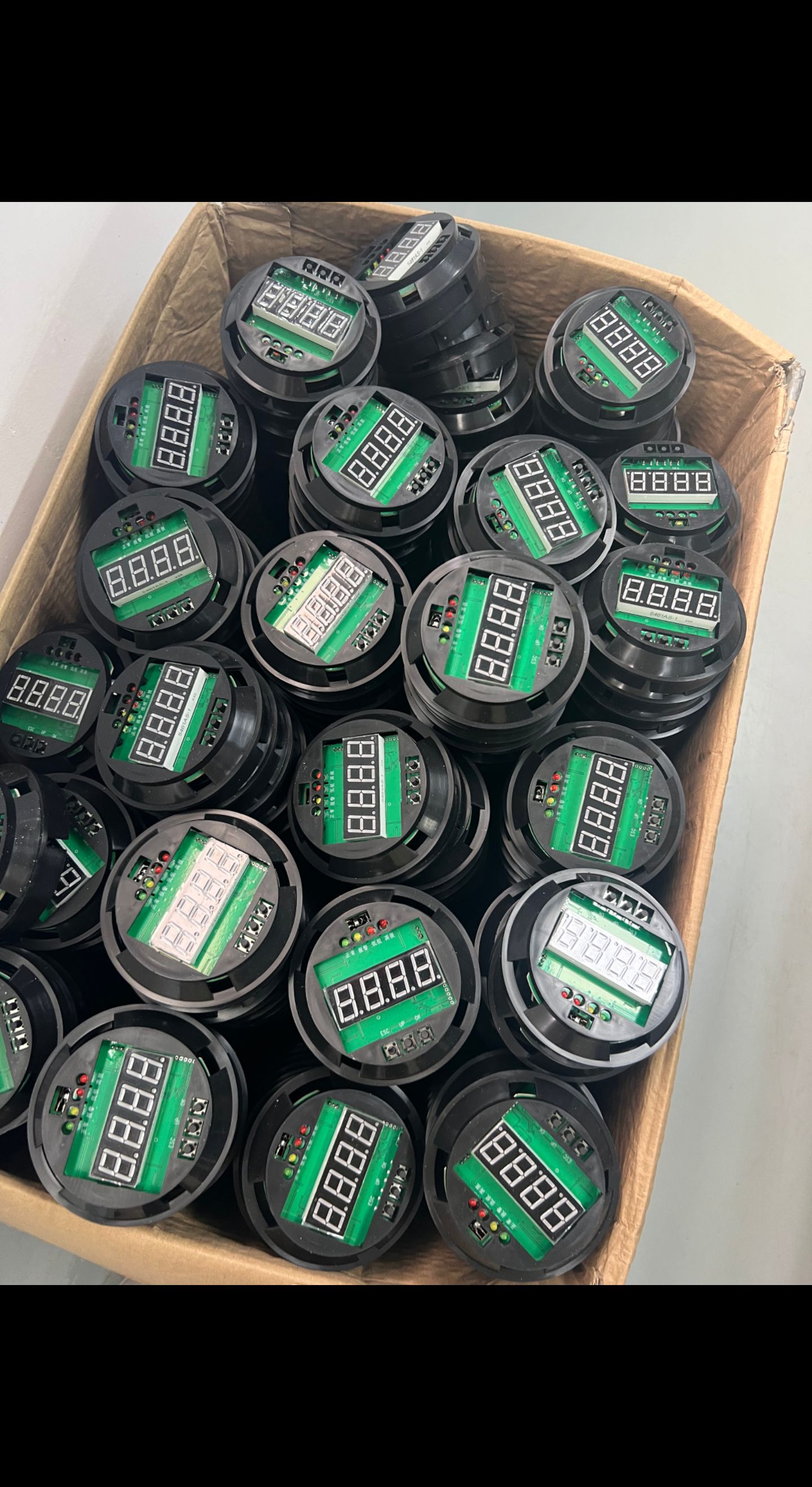
To put it simply, the process is: material selection, cutting, lamination, drilling, etching, solder mask application, surface treatment, shaping, testing, FQC, SMT (Surface Mount Technology) assembly, and PCBA (Printed Circuit Board Assembly) finished products.
10585 View