
Definition
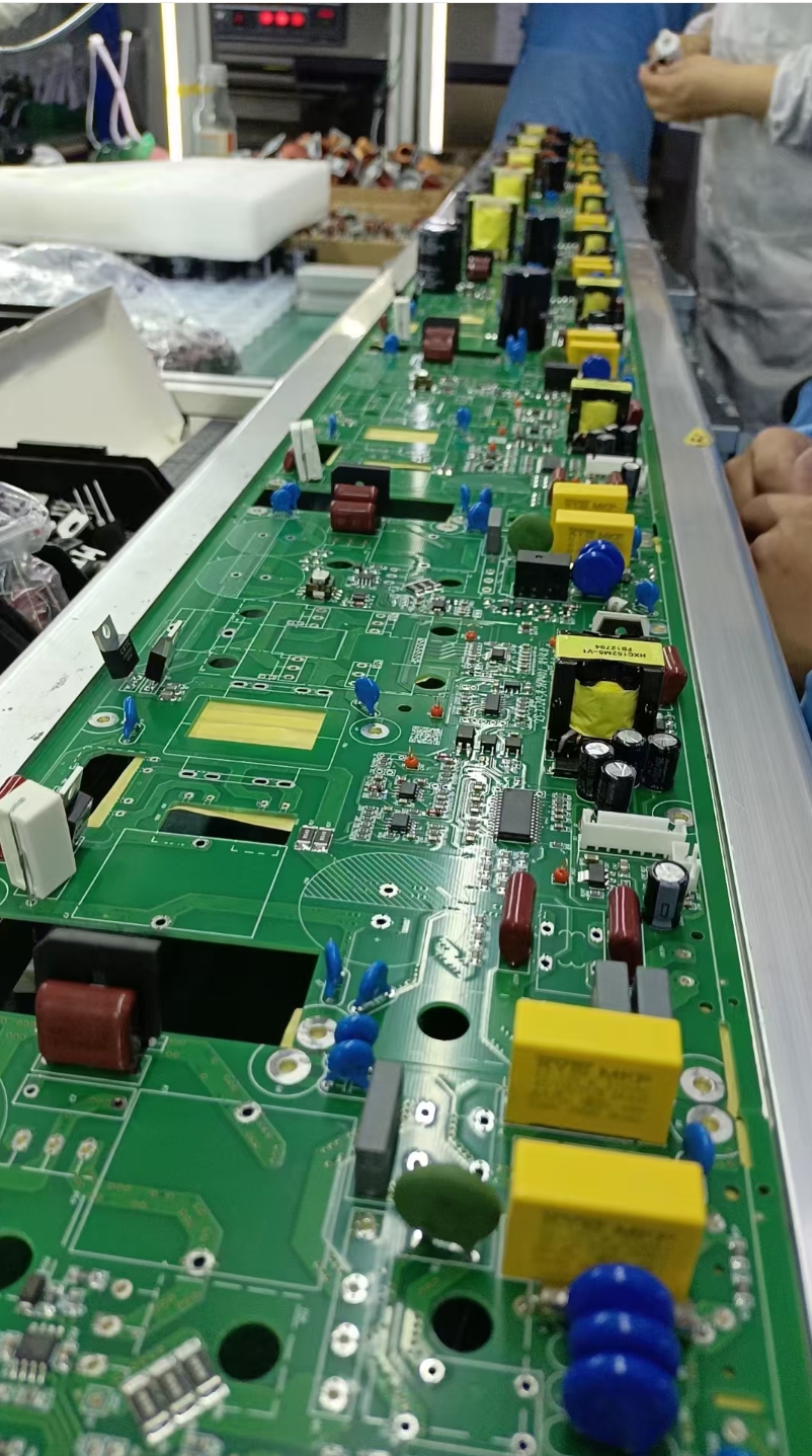
Multiple processed inner-layer circuit boards are bonded with semi-cured sheets (PP sheets), outer-layer copper foils, and other materials through high temperature and pressure to form a complete multi-layer printed circuit board.
Process
- Preparation: Blackening or brownening treatment is performed on inner-layer circuit boards to enhance their adhesion to semi-cured sheets. Meanwhile, semi-cured sheets and outer-layer copper foils are cut according to design requirements and cleaned.
- Stacking: Materials such as inner-layer circuit boards, semi-cured sheets, and outer-layer copper foils are stacked in a specific order, typically with semi-cured sheets sandwiched between inner-layer circuit boards and outer-layer copper foils.
- Lamination: The stacked board materials are placed into a laminator. Under high temperature (generally around 180°C) and high pressure (ranging from several to dozens of tons), after a certain period (usually tens of minutes), the semi-cured sheets melt to fill the gaps between layers, achieving close bonding between all layers.
- Cooling and Demolding: After lamination, the board is cooled to solidify and set its shape, then removed from the laminator to complete demolding.
Functions
- Electrical Connection: Through lamination, stable electrical pathways are formed between layers via the resin filling in semi-cured sheets and copper foil connections, ensuring accurate signal transmission between different layers.
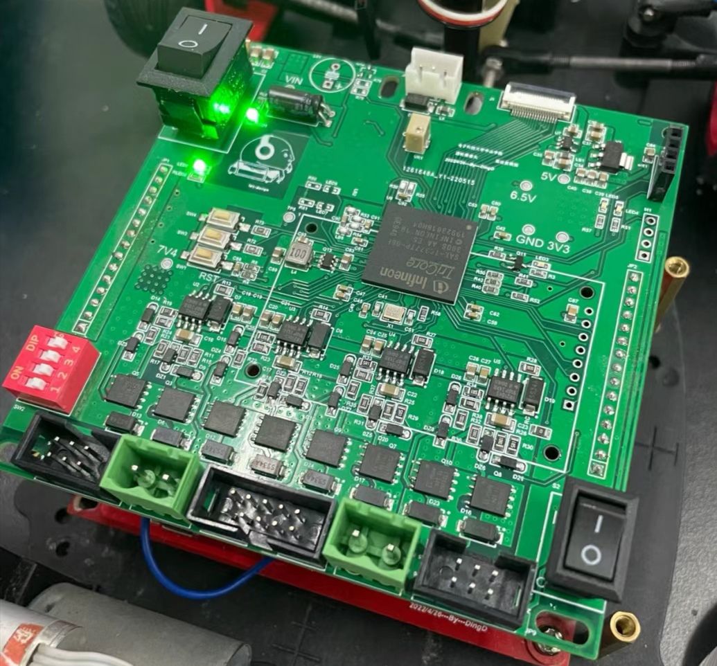
- Mechanical Support: Multi-layer circuit boards are integrated into a single unit, providing a stable mounting platform for electronic components and enhancing the mechanical strength of the PCB to withstand various external forces during the use of electronic devices.
- Circuit Protection: The protective layer formed by outer-layer copper foils and semi-cured sheets after lamination prevents inner-layer circuits from being eroded by the external environment, such as moisture, dust, and chemical substances, improving the reliability and service life of the PCB.
Quality Control
- Thickness Uniformity Control: Ensure that the thickness of the laminated PCB meets design requirements. Uneven thickness may cause difficulties in subsequent processing or affect circuit board performance.
- Prevention of Bubbles and Delamination: Strictly control lamination process parameters to avoid the generation of bubbles or delamination during lamination, which may affect the electrical and mechanical properties of the PCB.
- Dimensional Accuracy Assurance: Maintain the dimensional accuracy of the PCB during lamination to prevent issues such as board deformation and shrinkage, ensuring compatibility with other components.
10585 View