
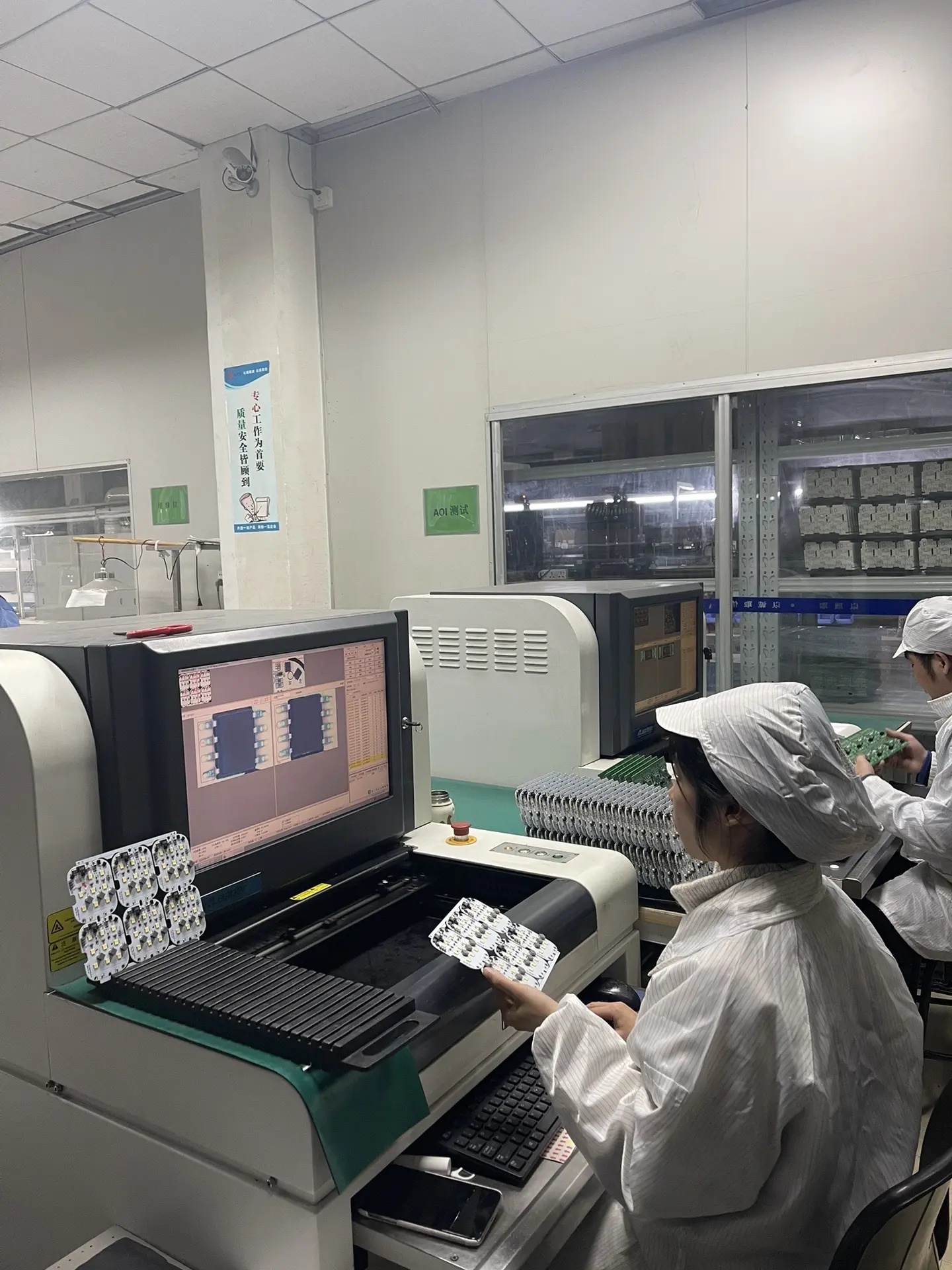
Working Principle
- Image Acquisition: High-resolution cameras scan the PCBA, with single or multiple lenses capturing comprehensive image information from different angles.
- Image Processing: The collected images are analyzed by software and compared with pre-set standard templates to identify key features such as component placement and solder joint morphology.
- Defect Recognition: Through comparison and analysis, common defects are identified, including solder joint defects, component placement errors, and other abnormalities on the circuit board surface.
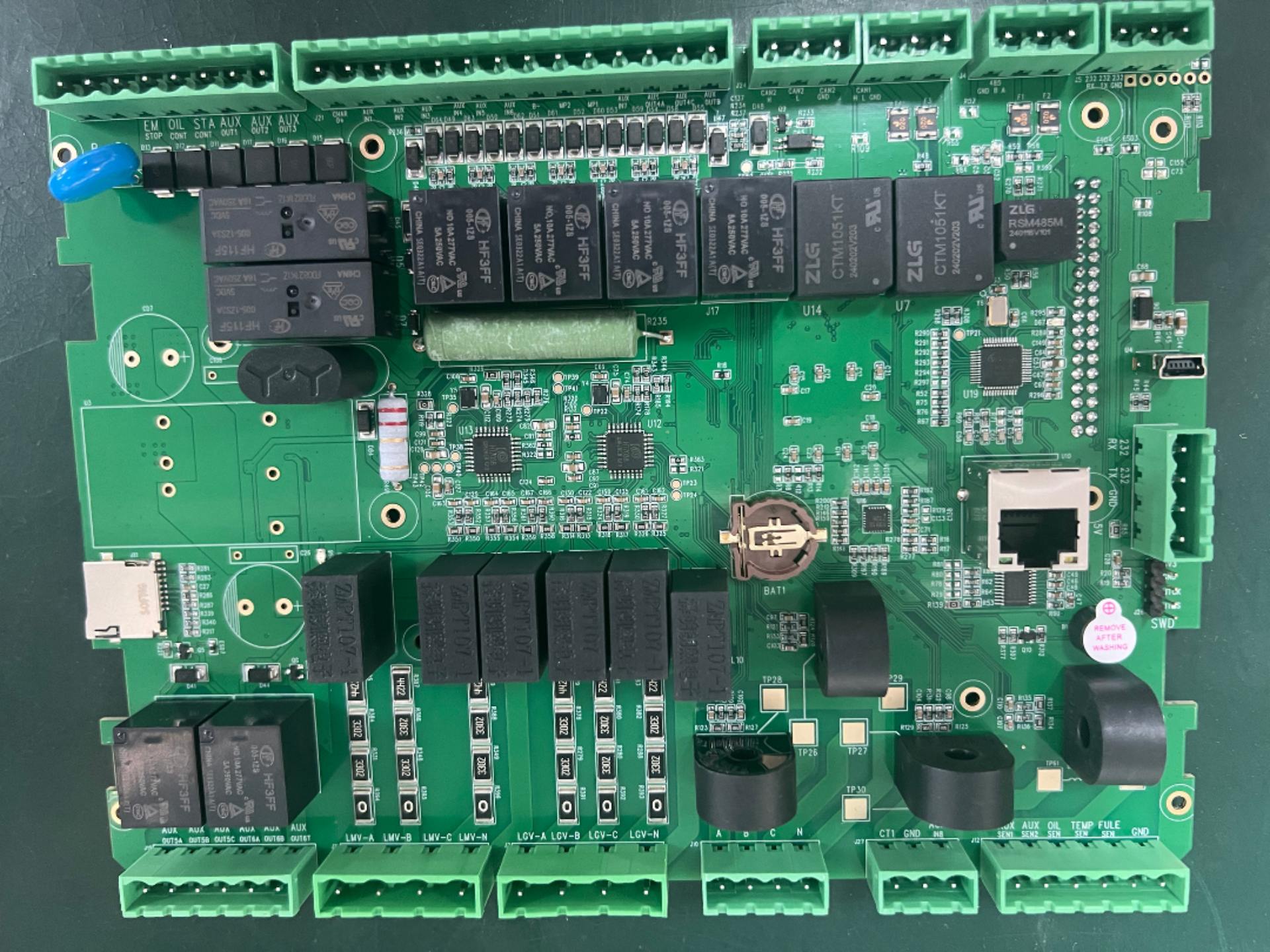
Inspection Content
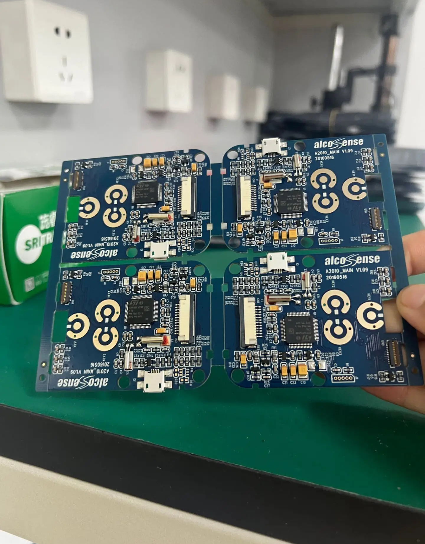
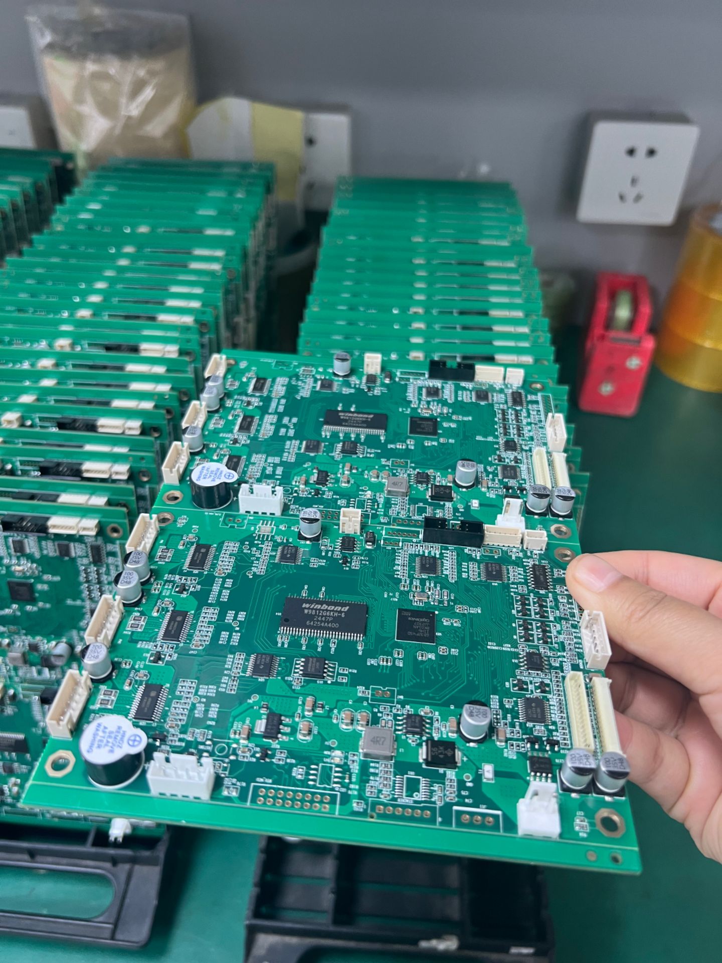
- Component Mounting Inspection: Detects issues such as missing components, misalignment, skewing, tombstoning, side-standing, flipped components, wrong components, damage, and reverse capacitor polarity.
- Welding Quality Inspection: Identifies solder defects like excessive/insufficient solder, cold solder joints, bridging, copper foil contamination, etc., and can infer welding strength through solder wetting status.
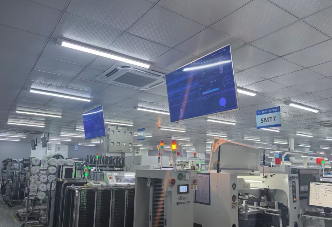
Equipment Classification
- By Inspection Mode: Divided into online AOI machines and offline AOI machines.
- By Position in Production Line: Includes AOI after screen printing, after component placement, after reflow soldering, and after wave soldering.
Advantages
- High Precision: Uses specialized detection algorithms and optical imaging processing to accurately identify tiny defects, avoiding human inspection errors.
- Fast Detection Speed: Equipped with high-speed systems, its speed is unaffected by PCB component density, enabling rapid inspection of large quantities of PCBA.
- Data Statistics and Analysis: Provides various production engineering statistics to analyze defect causes and optimize production processes.
10585 View