
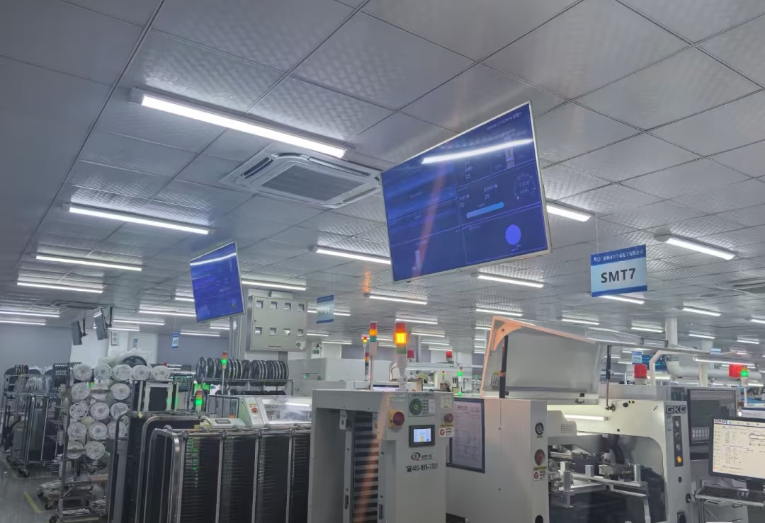
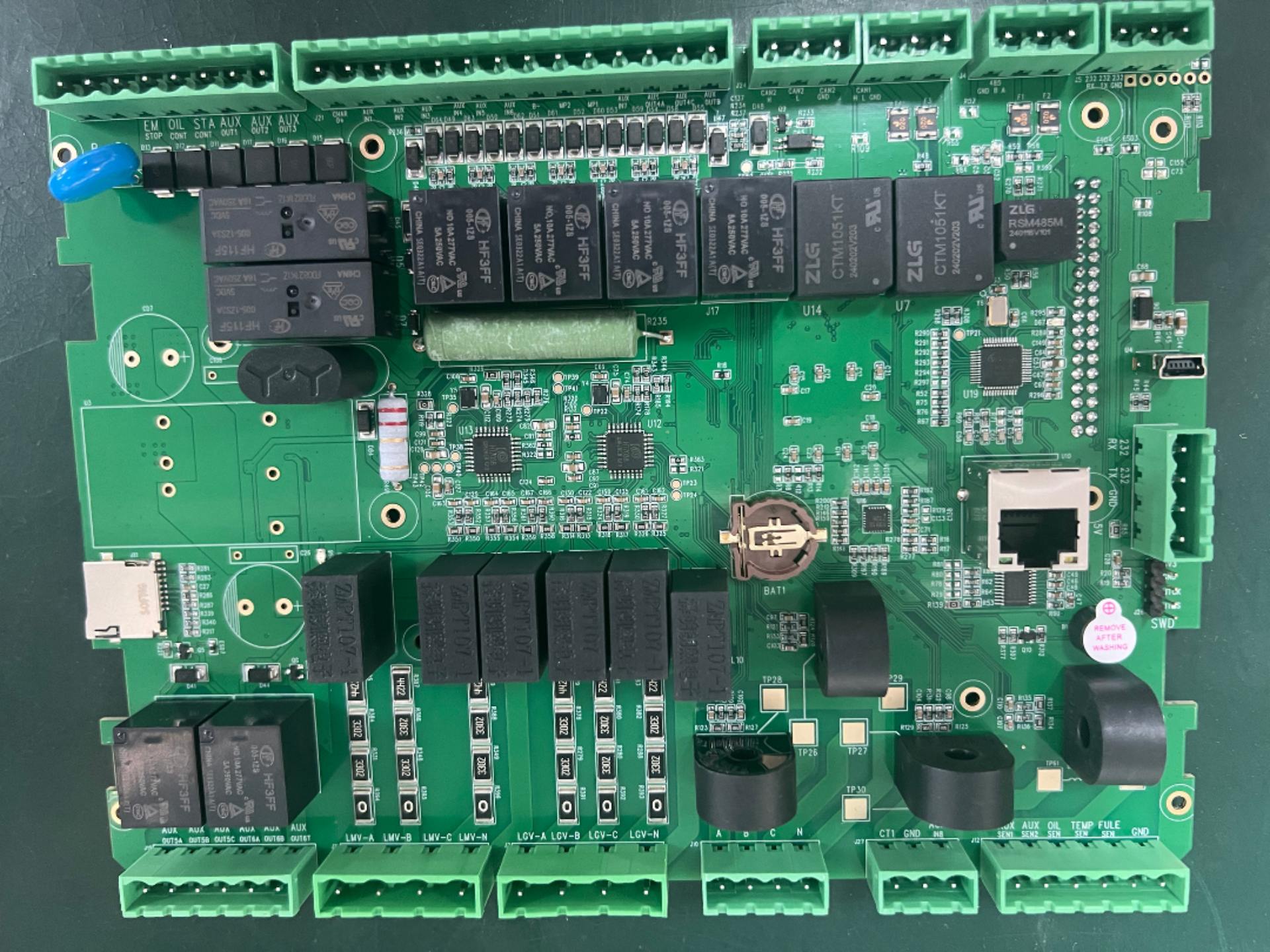
PCB hole tolerances (diameter & position) directly impact board precision, reliability, and cost, with drilling processes being the core influence factor. Here’s the condensed guide:
1. Hole Diameter Tolerance: Drilling Method is King
- Mechanical Drilling
- Application: Standard through-holes, larger blind/buried holes
- Tolerance range: ±0.05–0.10mm (high-precision drills hit ±0.05mm)
- Key factors: Drill bit quality/wear, stack layer count & material uniformity, spindle stability, cover/back-up plate selection
- Laser Drilling
- Application: Micro-holes (<0.15mm), HDI boards
- Tolerance range: CO₂ laser ±0.025–0.05mm; UV laser up to ±0.01mm (best precision, minimal thermal impact)
- Key factors: Laser energy/pulse stability, alignment accuracy, material laser absorption rate
2. Hole Position Tolerance: Alignment & Drilling Precision Matter Most
- Drilling Process Accuracy
- Mechanical drilling: ±0.015mm (high-end machines), affected by material expansion/contraction, machine thermal expansion, drill bit slippage
- Laser drilling: ±0.005mm (UV laser), non-contact positioning & LDI data linkage reduce errors
- Interlayer Alignment Methods (Critical for Multilayer Boards)
- Target alignment: Widely used for standard boards, tolerance affected by lamination misalignment (0.05–0.15mm offset) & optical recognition errors
- X-RAY alignment: HDI board standard, detects inner-layer targets directly, cuts tolerance to ±0.025mm
- Laser direct ablation alignment: Aligns with inner pads via CCD, precision below ±0.01mm for micro-via alignment
Pro Tip
Choose drilling & alignment methods based on PCB density requirements—HDI boards demand UV laser drilling + X-RAY/CCD alignment for optimal precision.
10585 View