
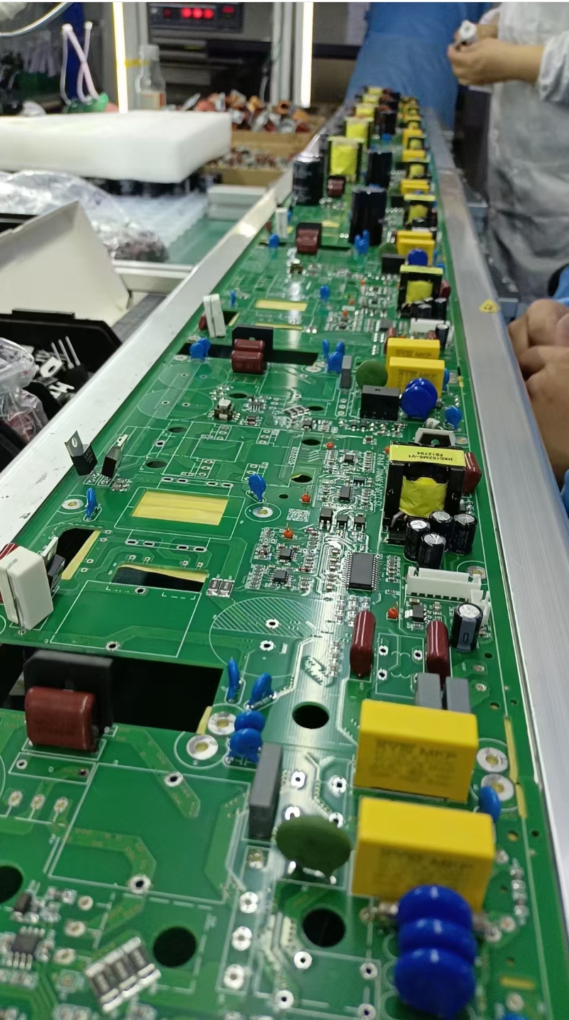
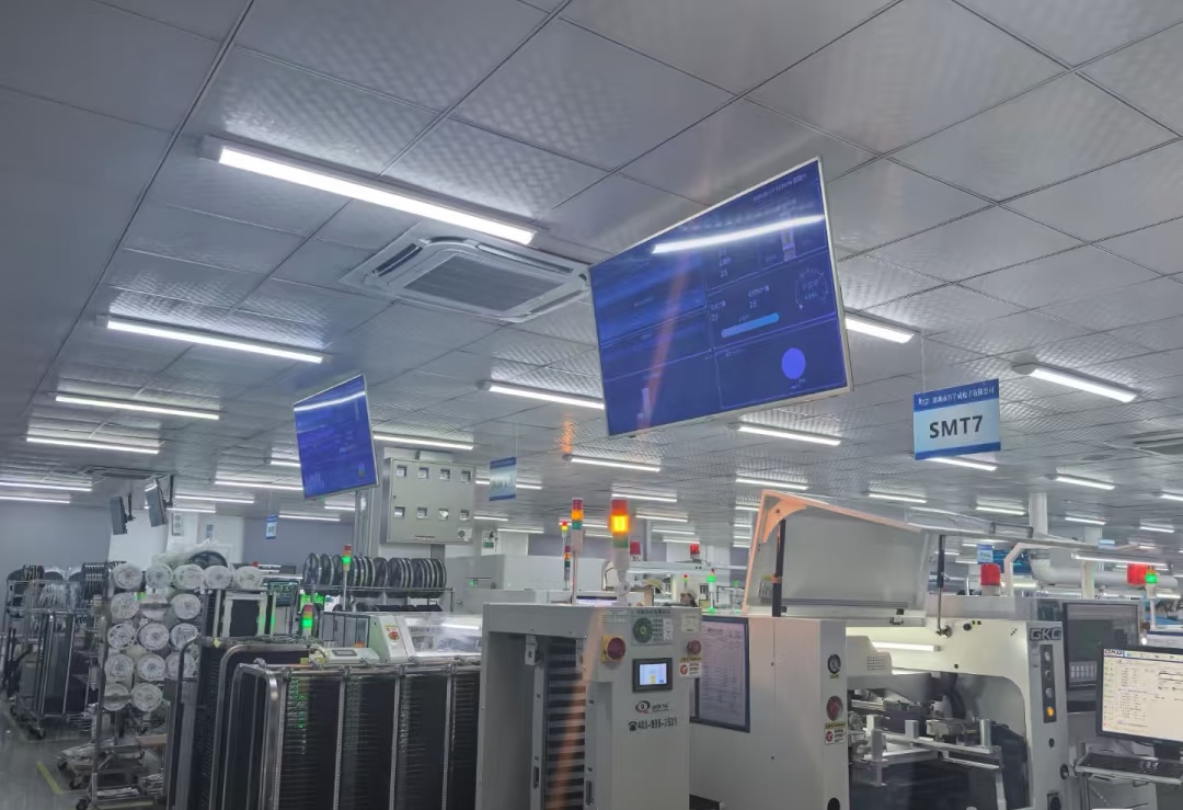
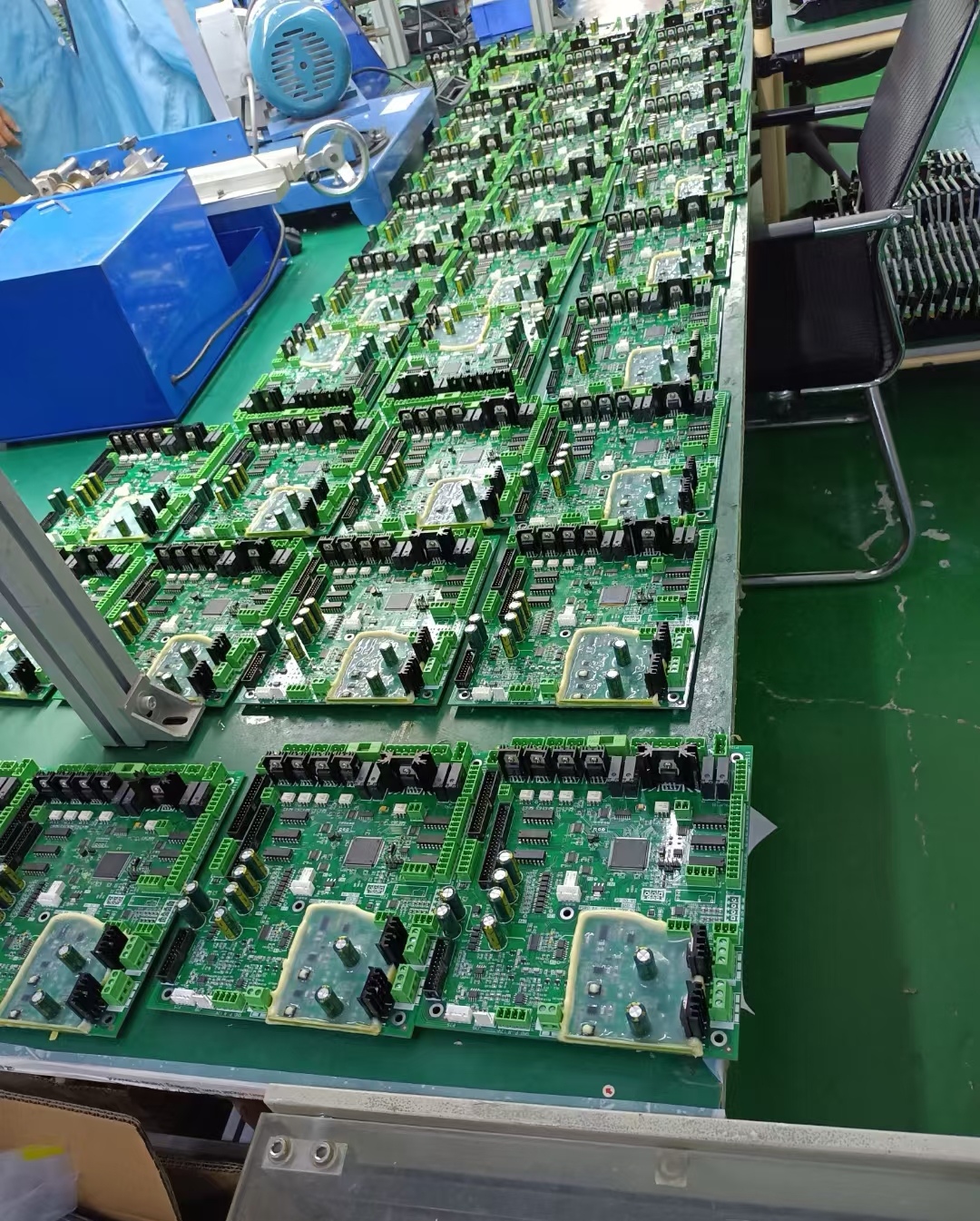
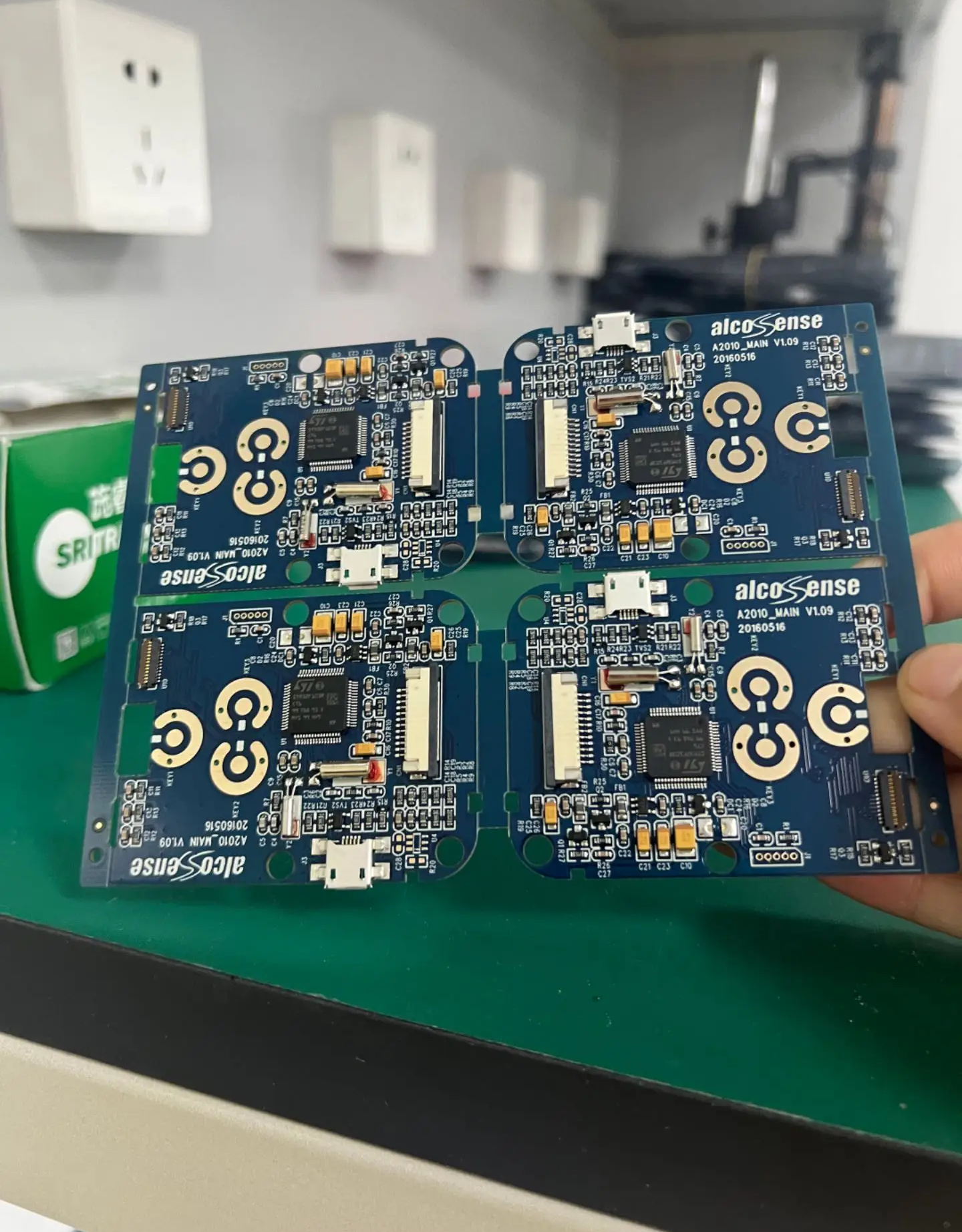
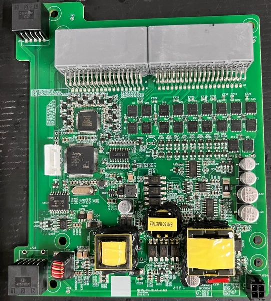
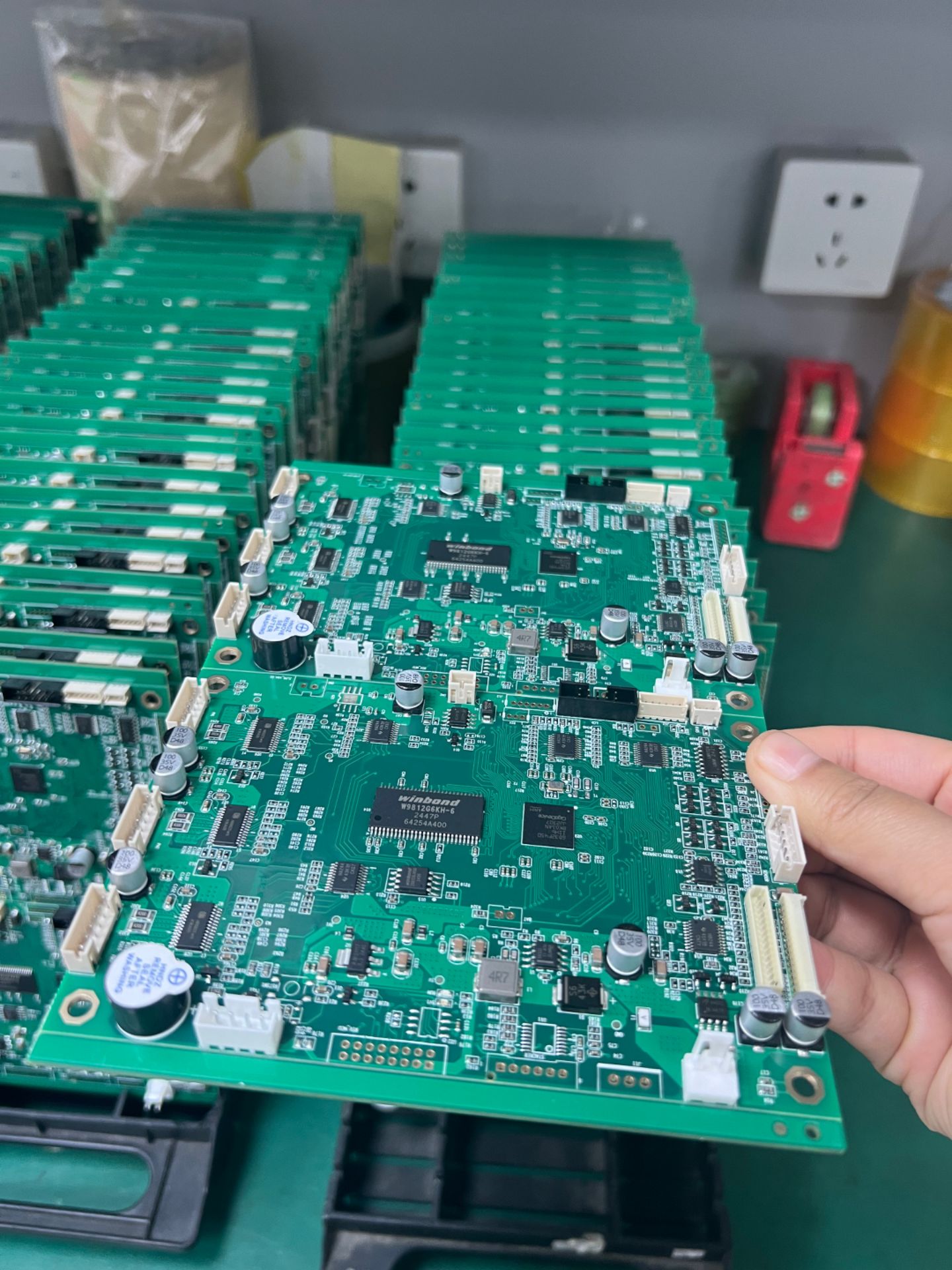
In high-power equipment, industrial control, automotive electronics and other fields, the demand for PCBs thicker than 3.0mm (even up to 4.0mm or 6.0mm) is growing. Crossing this thickness threshold, however, pushes PCB fabrication from conventional processes into the realm of thick/ultra-thick board manufacturing, accompanied by a host of process challenges.
Sharing frontline manufacturing experience to break down the core challenges and solutions for thick board production👇
I. Core Pain Points of Thick PCB Fabrication
1. Machining: Exponentially Increased Difficulty
- Drilling Issues: Deeper holes lead to poor chip evacuation and frequent drill breakage; excessive aspect ratio causes hole deviation and misalignment between inner and outer layers; hole walls are prone to smear, roughness and even "bell-mouth" defects.
- Forming Bottlenecks: Traditional V-CUT has limited depth, unable to adapt to thick board depaneling—forced separation leads to edge chipping and cracking; routing accelerates cutter wear, resulting in burrs, delamination and corner chipping on edges.
2. Lamination: Dual Challenges of Thermal Stress and Resin Filling
- Insufficient Resin Filling: Longer resin flow paths of prepregs cause "resin starvation" or voids in inner-layer drilled areas, significantly reducing interlayer adhesion.
- Bubble and Delamination Risks: Trapped air and volatiles in thick boards are hard to discharge, forming bubbles under high temperature and pressure, which trigger delamination after cooling.
- Warpage: Thermal stress from CTE differences of materials is amplified in thick boards, leading to warpage that disrupts subsequent SMT assembly.
3. Electroplating: Major Challenge of Copper Uniformity in Holes
Electroplating solution struggles to penetrate deep holes evenly, resulting in "dog bone" or "waist drum" effects (adequate copper thickness at hole ends but insufficient in the middle), which impairs current-carrying capacity and reliability; filling blind/buried vias in HDI thick boards becomes exponentially harder.
4. Assembly & Soldering: Hidden Reliability Thresholds
- Poor Solder Penetration: Limited heat conduction during wave soldering or manual soldering causes voids in hole middles, reducing solder joint mechanical strength and electrical connection reliability.
- Unstable Component Mounting: Heavy components fixed only by solder joints are prone to fatigue fracture under vibration.
5. Equipment & Materials: Hard Constraints
Most automated production equipment (conveyor tracks, exposure machines, etching lines) has a thickness limit (typically ≤3.2mm); high-reliability substrates with high TG and low CTE are required, leading to higher costs.
II. Solutions: Key Strategies for Thick PCB Fabrication
1. Optimize Machining Processes
- Drilling: Adopt peck drilling for chip evacuation and heat dissipation; use high-rigidity tungsten carbide drills with optimized speed and feed rate; drill pilot holes first then ream, strictly controlling aspect ratio (recommended ≤10:1).
- Forming: Replace V-CUT with routing or breakaway tabs for depaneling; use slower routing speed, multiple passes and new cutters to improve edge quality; adopt depth-controlled routing for ultra-thick boards.
2. Improve Lamination to Control Thermal Stress
- Use low-flow or high-resin-content prepregs to ensure sufficient filling.
- Adopt multi-stage heating/pressurization lamination profiles, extending low-temperature holding time for full resin flow and gas release before high-pressure curing.
- Add buffer materials and resin flow channels to guide excess resin and gas discharge.
- Implement post-lamination baking to eliminate internal stress and reduce warpage.
3. Upgrade Electroplating Technology for Hole Copper Quality
- Adopt pulse plating or horizontal plating to enhance electrolyte exchange in deep holes and improve copper uniformity.
- Equip strong agitation devices like ultrasonic vibration to assist electrolyte penetration.
- Extend plating time and conduct destructive cross-section analysis to monitor hole copper thickness throughout production.
4. Collaborate on Design & Manufacturing to Reduce Difficulty from the Source
This is the most efficient way to tackle thick board challenges. Conduct DFM analysis with manufacturers early:
- Relax design tolerances, increasing line width/space, hole diameter and pad size.
- Optimize hole design, avoiding overly small apertures to leave process margin for electroplating.
- Add process edges and tooling holes to improve production positioning accuracy.
- Consider back drilling for high-speed signals to remove redundant copper stubs and enhance electrical performance.
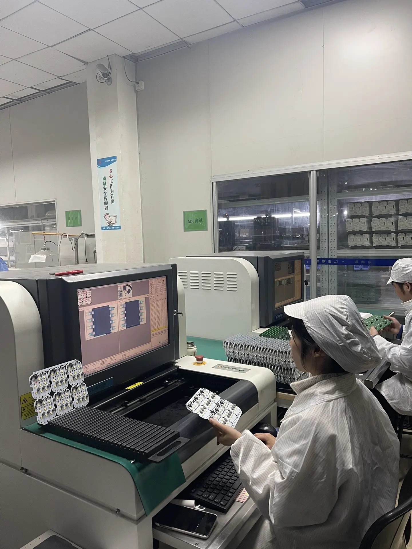
5. Strengthen Quality Control to Ensure Reliability
- Perform 100% electrical continuity testing to eliminate open-circuit risks.
- Increase cross-section analysis frequency to monitor hole copper quality and interlayer adhesion.
- Use 3D X-Ray for non-destructive testing of internal copper and layer alignment.
- Conduct thermal stress tests (e.g., 288℃ solder dip test) to verify via plating and lamination reliability.
III. Conclusion
The core challenge of thick PCB fabrication lies in the reduced uniformity and controllability of physical and chemical processes due to increased thickness.
Key Advice: Engage with manufacturers experienced in thick board production at the early stage of demand definition and conduct DFM analysis upfront. Note that thick board production requires longer lead times and higher costs than standard boards—set reasonable expectations.
10585 View