
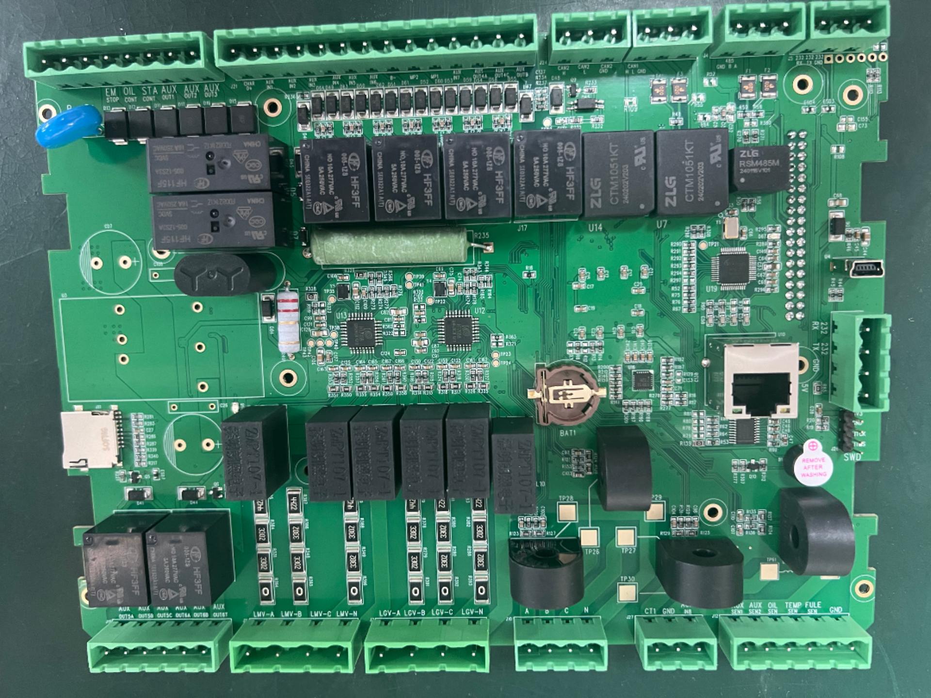
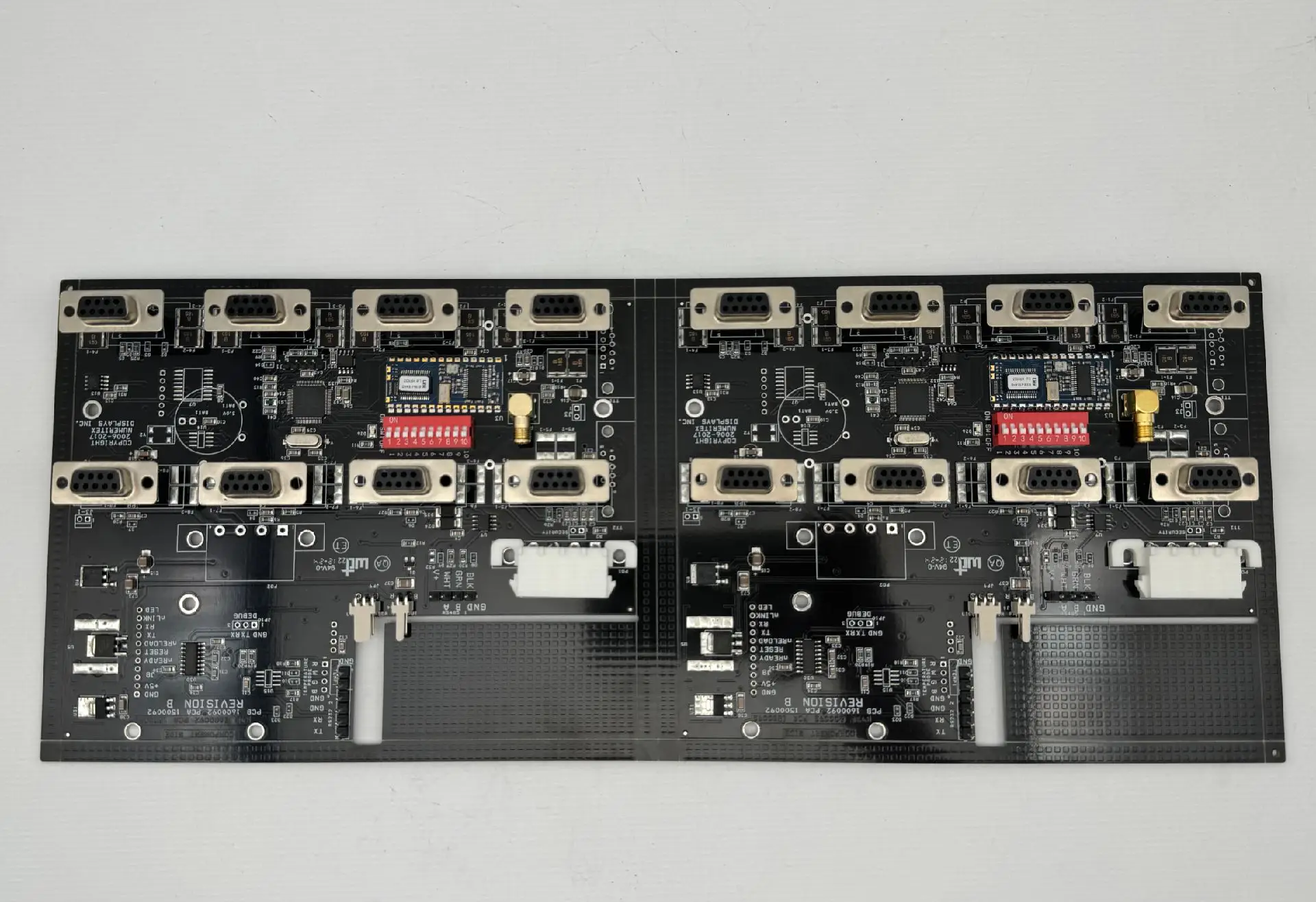
Many customers requiring PCBA processing often ask: "I only have a circuit diagram—can I place an order for processing?" The answer is a definite no. To ensure the smooth progress of PCBA OEM/ODM services, from prototyping to mass production, a full set of complete PCBA processing and production documentation must be prepared in advance. Incomplete documentation can, at best, cause delivery delays; at worst, it may lead to component placement errors and even the scrapping of entire circuit boards.
Below is a breakdown of the essential documentation required for PCBA processing.
1. Bill of Materials (BOM) – The "Instruction Manual" for Component Procurement
The BOM is the most fundamental and critical document, used for component sourcing, alternative part verification, and placement material scheduling. It should include the following details:
- Reference Designator
- Part Name
- Package Type
- Value/Specifications
- Manufacturer & MPN (Manufacturer Part Number)
- Placement Location
- Critical Component Indicator (optional)
- Recommended Alternative Parts (optional)
Note: It is best to present the BOM in Excel format. Clearer information will improve the OEM factory’s procurement efficiency and reduce error rates.
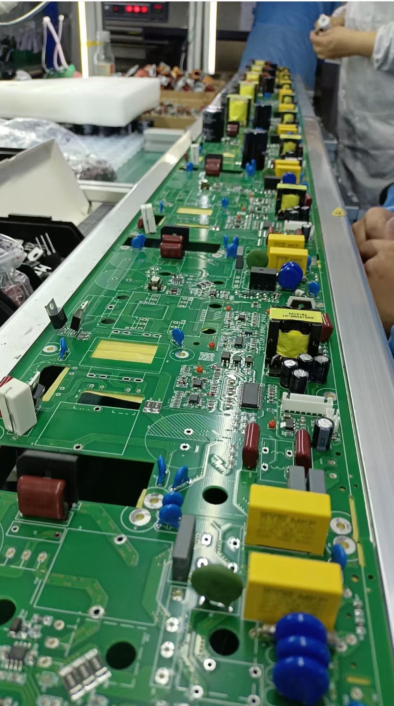
2. Gerber Files (PCB Manufacturing Data) – The "Blueprint" of the Circuit Board
Gerber files are the standard file format for PCB fabrication, controlling processes such as etching, solder mask opening, and electroplating. They must include the following layers:
- Top Layer
- Bottom Layer
- Solder Mask
- Silkscreen Layer
- Drill Drawing
- NC Drill File
Recommendation: Export Gerber files in RS-274X format and attach the drill information ( .drl file) to ensure precise PCB manufacturing.
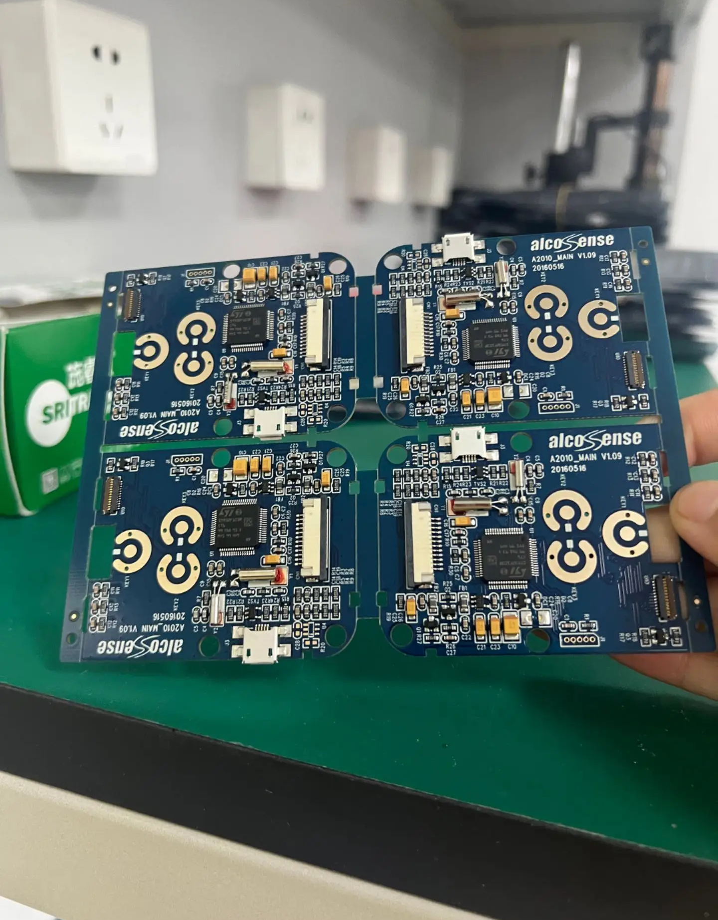
3. Pick and Place File – The "Navigation Map" for SMT Placement
Pick and place files are used by SMT placement machines to position components accurately. They typically include:
- Component Reference Designator (Ref.)
- Component Center Coordinates (X, Y)
- Rotation Angle
- Layer Information (Top/Bottom)
This file is usually exported automatically by PCB design software, but OEM factories can also assist with its creation if needed.
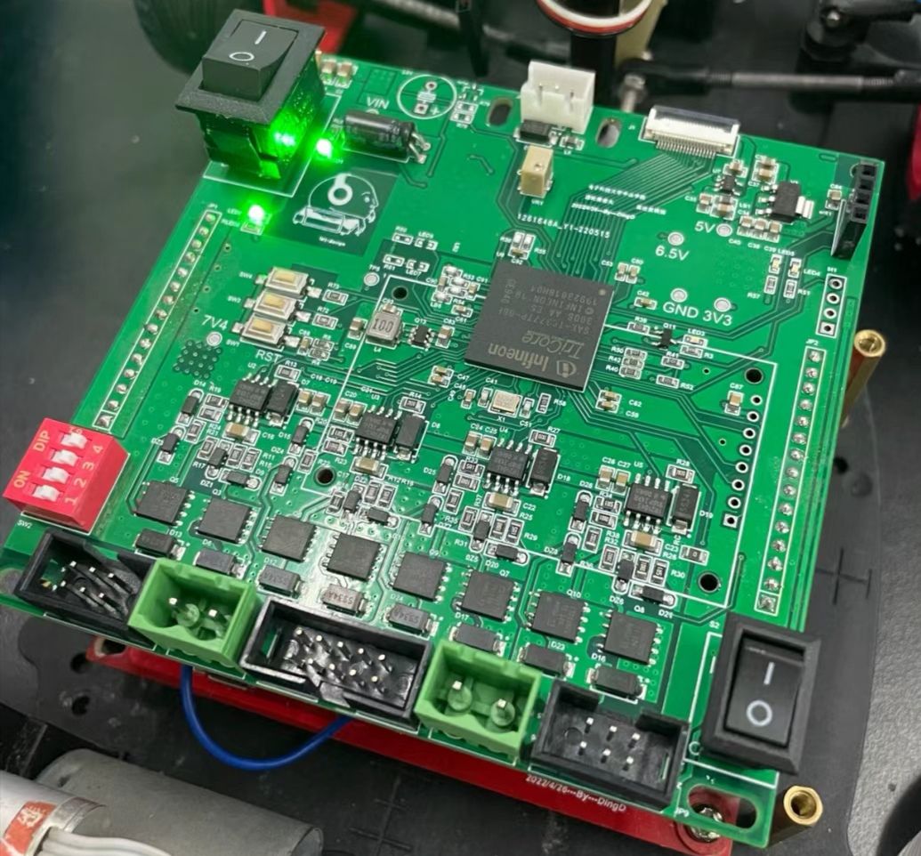
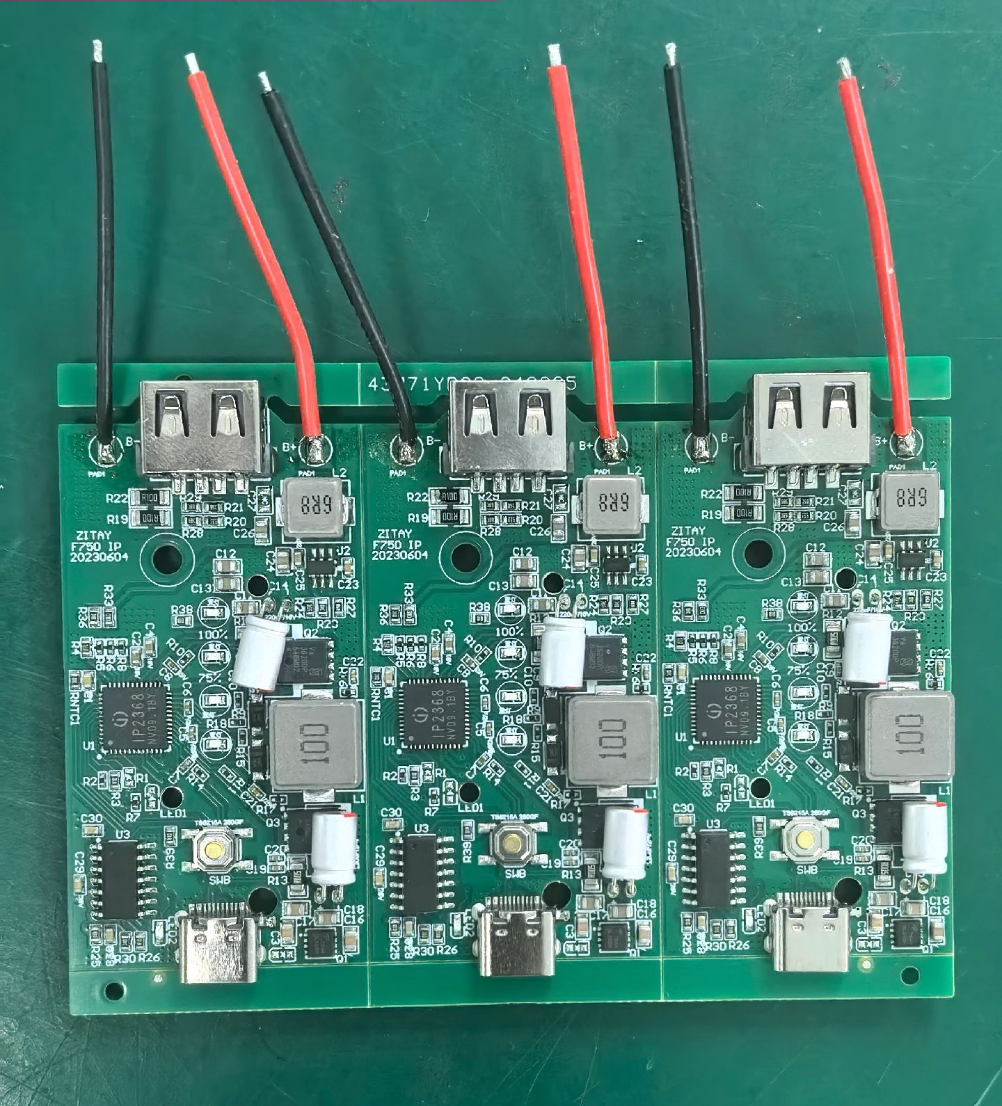
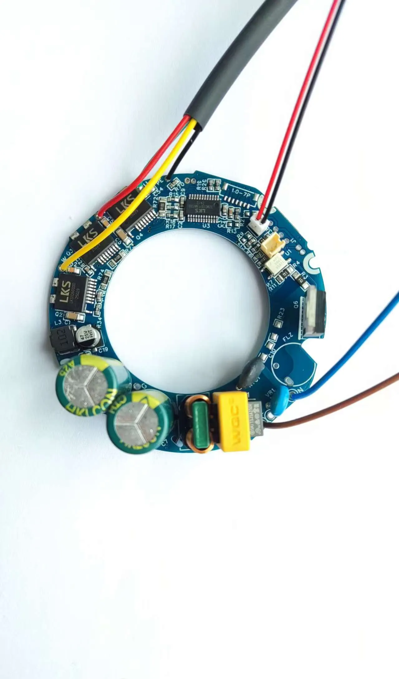
4. Assembly Drawings & Instructions – Avoid Misunderstandings and Omissions
While Gerber files and BOMs are essential, assembly drawings or detailed enlarged views are also indispensable. They help assemblers and inspectors quickly identify critical components and polarity-sensitive devices (e.g., polarized capacitors, LEDs, ICs).
In addition, please specify any special process requirements in advance, such as potting, selective solder mask, or selective wave soldering.
5. Test Plan or Test Point Drawings (if applicable) – Ensure Delivery Yield
For customers requiring functional testing, ICT (In-Circuit Testing), or FCT (Functional Circuit Testing), please provide the corresponding test plan, test point information, or fixture design drawings. This allows for advance negotiation of test conditions and avoids post-production discrepancies.
6. PCB Material Parameters (if providing PCBs yourself) – Ensure Process Compatibility
If customers supply their own PCBs, they must specify the material type (e.g., FR4, high TG), number of layers, board thickness, copper thickness, tolerances, and surface finish (e.g., OSP, HASL, ENIG). These parameters determine the settings for the placement process.
7. Critical Component Instructions & Substitution Requirements (if applicable)
If certain components have designated brands or are non-substitutable, please clearly indicate this in the BOM. Conversely, if domestic alternative parts are acceptable, specify this as well—it helps OEM factories control costs and ensure on-time delivery.
8. Additional Supplementary Documentation (based on project requirements)
Examples include:
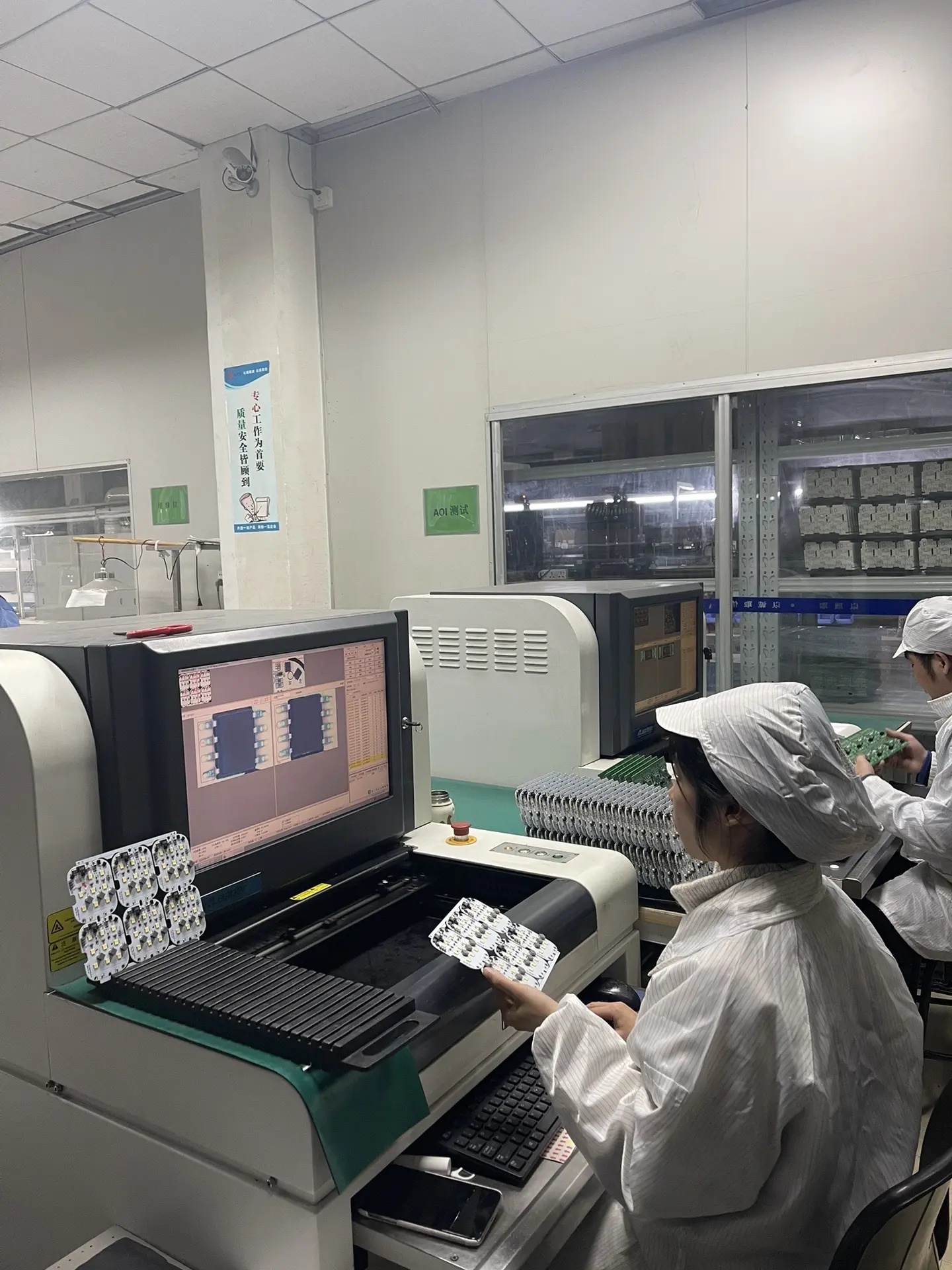
- SPI (Solder Paste Inspection) thickness requirements
- AOI (Automated Optical Inspection) acceptance standards
- Packaging requirements (e.g., blister trays, pallets, anti-static bags)
- Barcode printing specifications
These details may seem minor, but they are crucial for mass delivery.
Frequently Asked Questions (FAQs)
Q1: Can I place an order if my PCBA processing documentation is incomplete?
Generally, it is not recommended. Incomplete documentation increases the risk of placement errors and poor soldering. Reputable OEM factories will always require full documentation before confirming production.
Q2: Are BOMs, Gerber files, and pick and place files provided by the customer, or can the manufacturer assist with creating them?
In most cases, these documents are provided by the customer. However, if you only have a schematic diagram, the manufacturer can assist with BOM compilation, Gerber file export, and pick and place file creation.
Q3: Are the documentation requirements the same for SMT prototyping and mass production?
The requirements are basically the same. However, some assembly drawings or test documentation can be omitted during the prototyping phase. For mass production, it is recommended to complete all documentation to ensure product consistency.
Complete documentation = Efficient processing = High-quality products!
PCBA processing is not a simple matter of "sending a schematic and waiting for delivery"—it is a highly collaborative engineering process. Preparing full documentation is the first step to ensuring on-time delivery, cost control, and high yield rates.
10585 View