
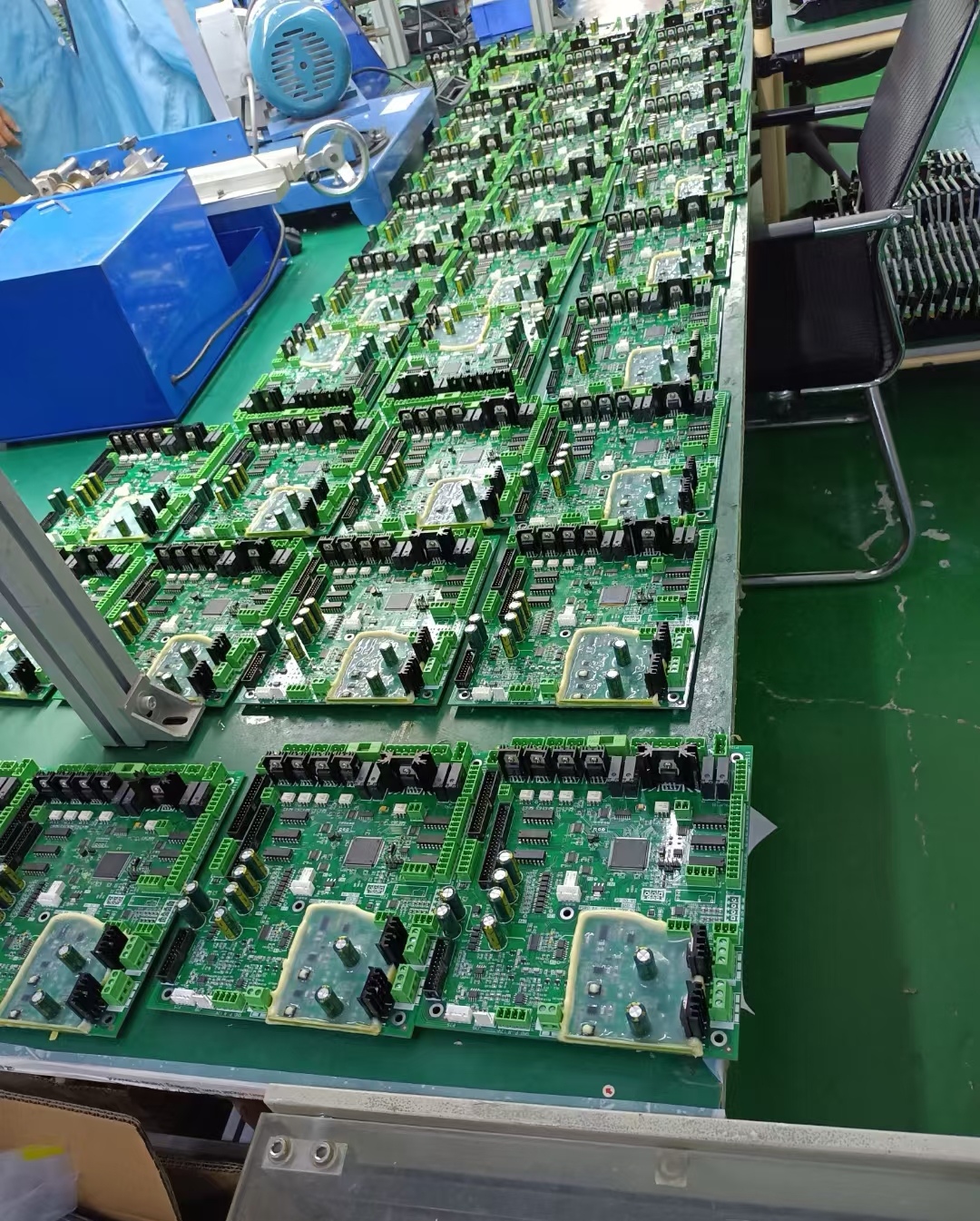
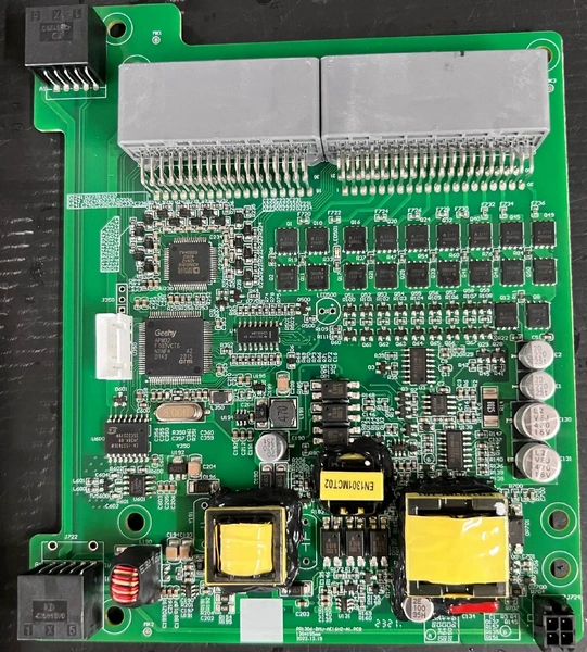
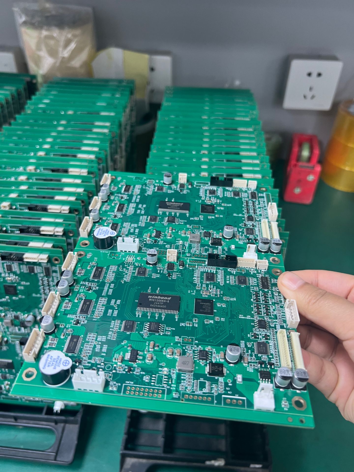
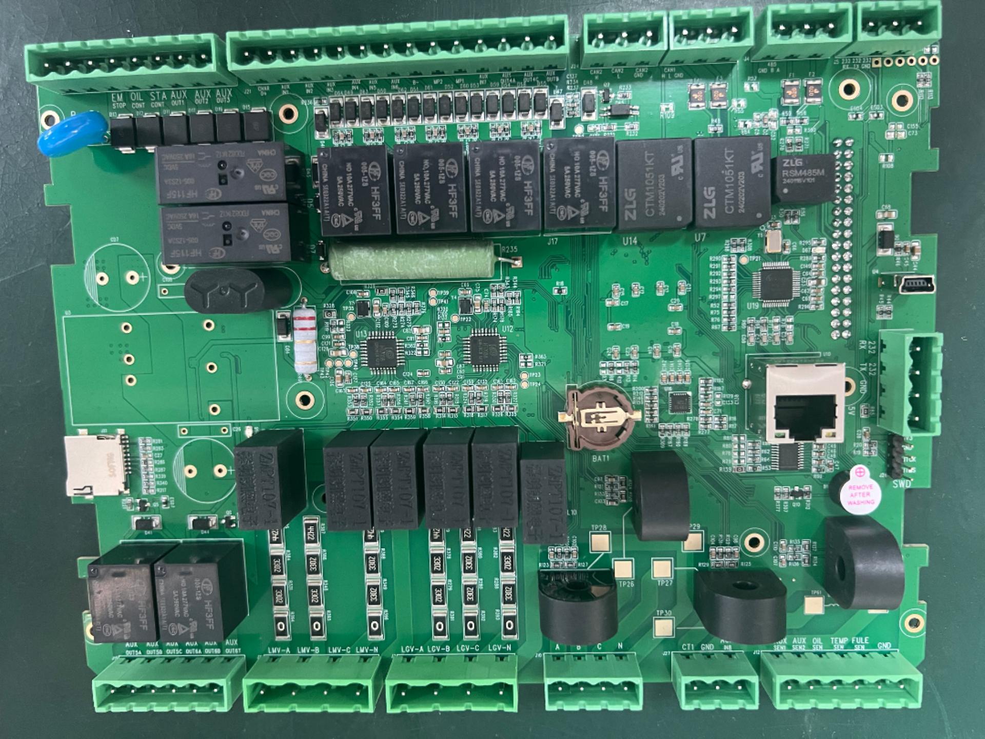
Have You Ever Encountered This Situation: A PCB Crashes as Soon as It’s Powered On, and Communication Is a Complete Mess!
In fact, the problem often lies in routing. Many engineers only remember two key rules after falling into pitfalls.
The first is the 3W Rule: The center-to-center spacing between high-speed signal traces must be ≥ 3 times the trace width. For example, if the trace width is 5 mils, the spacing should be at least 15 mils to effectively reduce crosstalk.
The second is the 20H Rule: The size of the power plane should be 20 times the dielectric thickness smaller than the ground plane. If the dielectric thickness is 0.2 mm, the power plane must be 4 mm smaller than the ground plane. This helps reduce EMI radiation interference.
Don’t underestimate these two rules—they can truly determine whether the board operates stably or "fails as soon as it’s powered on".
What pitfalls have you encountered during PCB routing? Feel free to share in the comments section.


10585 View