
The lamination process of multi-layer PCB circuit boards is a complex but important process that involves ensuring precise alignment and strong bonding between the layers of the circuit board. The following are the general processing steps:
Material preparation: First of all, it is necessary to prepare the materials used to make the circuit board, including the circuit board substrate, copper foil, prepreg, etc. These materials need to undergo strict quality inspection to ensure that they meet the production requirements.
Board production: According to the designed circuit board graphics, negative production and circuit production are carried out. Negative production is to transfer the circuit board graphics to the circuit board substrate, while circuit production is to cover copper foil on the negative film, and through exposure, Development and other process steps form a circuit board.
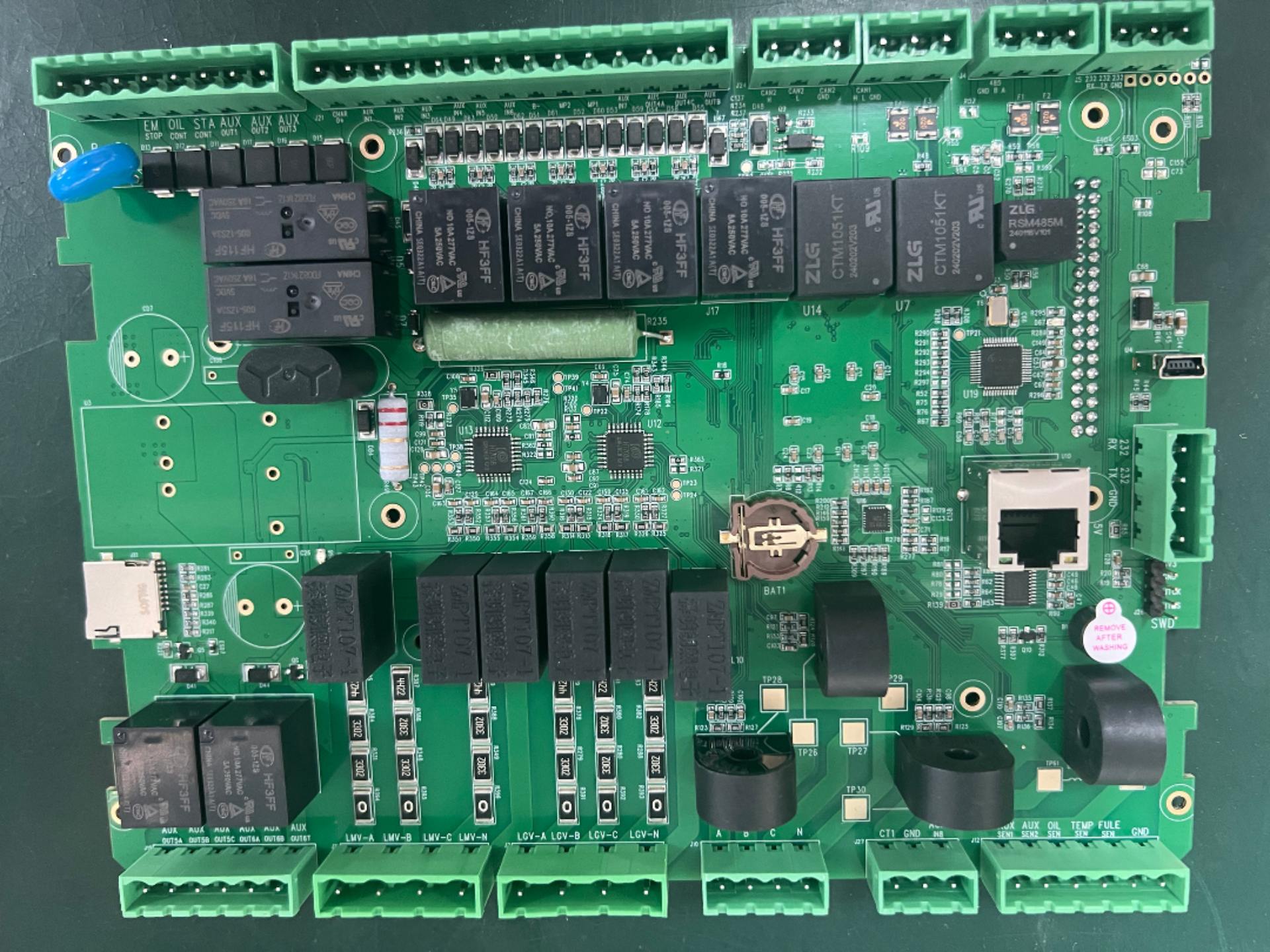
Lamination and positioning: Stack and position individual circuit board substrates according to design requirements. This process requires ensuring precise alignment between the layers to ensure the functionality and performance of the circuit board.
Pre-pressing: After lamination and positioning are completed, a pre-pressing process is required. The purpose of pre-pressing is to initially bond the layers for subsequent formal pressing.
Formal lamination: Put the pre-pressed circuit board into the laminator for formal lamination. During the lamination process, parameters such as temperature, pressure and time need to be controlled to ensure that the adhesion between the layers reaches the expected requirements. At the same time, attention should also be paid to using appropriate cushioning materials (such as kraft paper) to protect the circuit board and prevent it from being damaged during the lamination process.
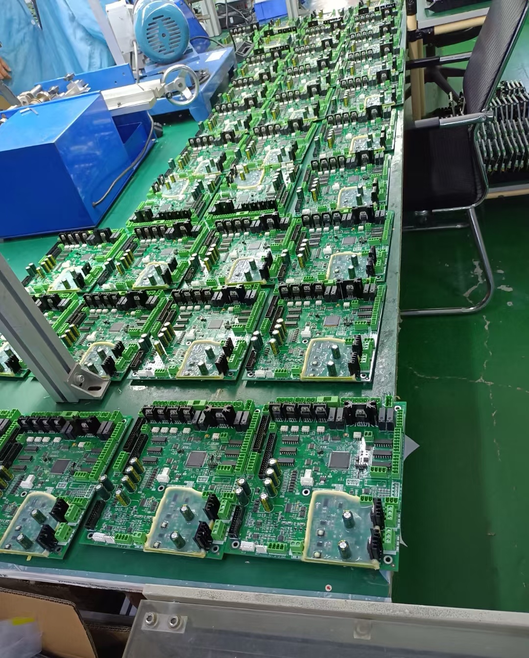
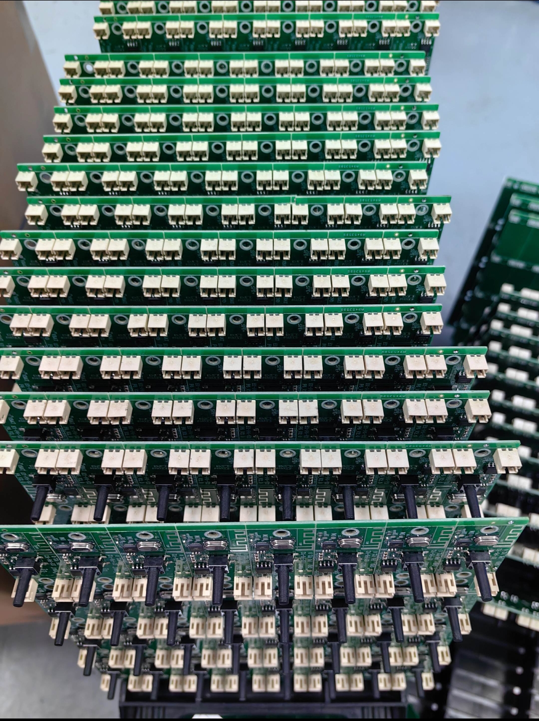
Machining and Drilling: After the pressing is complete, the circuit board needs to be machined and drilled to form the desired shape and connection holes.
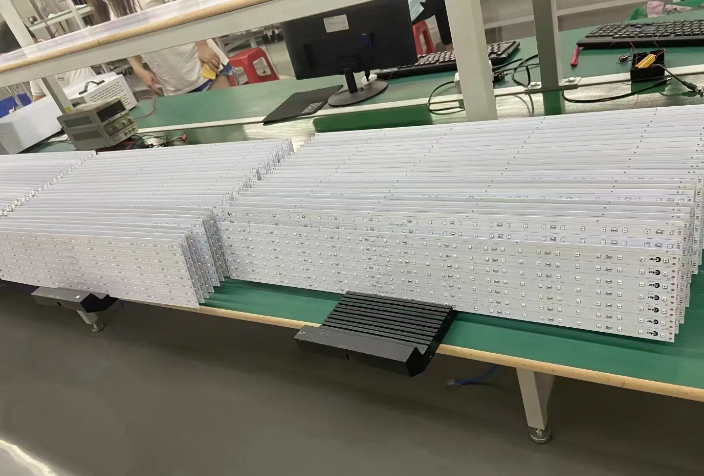
Surface Treatment: The surface of a circuit board is treated to enhance its electrical conductivity and reliability. This usually involves applying a protective lacquer or performing other surface treatment processes.
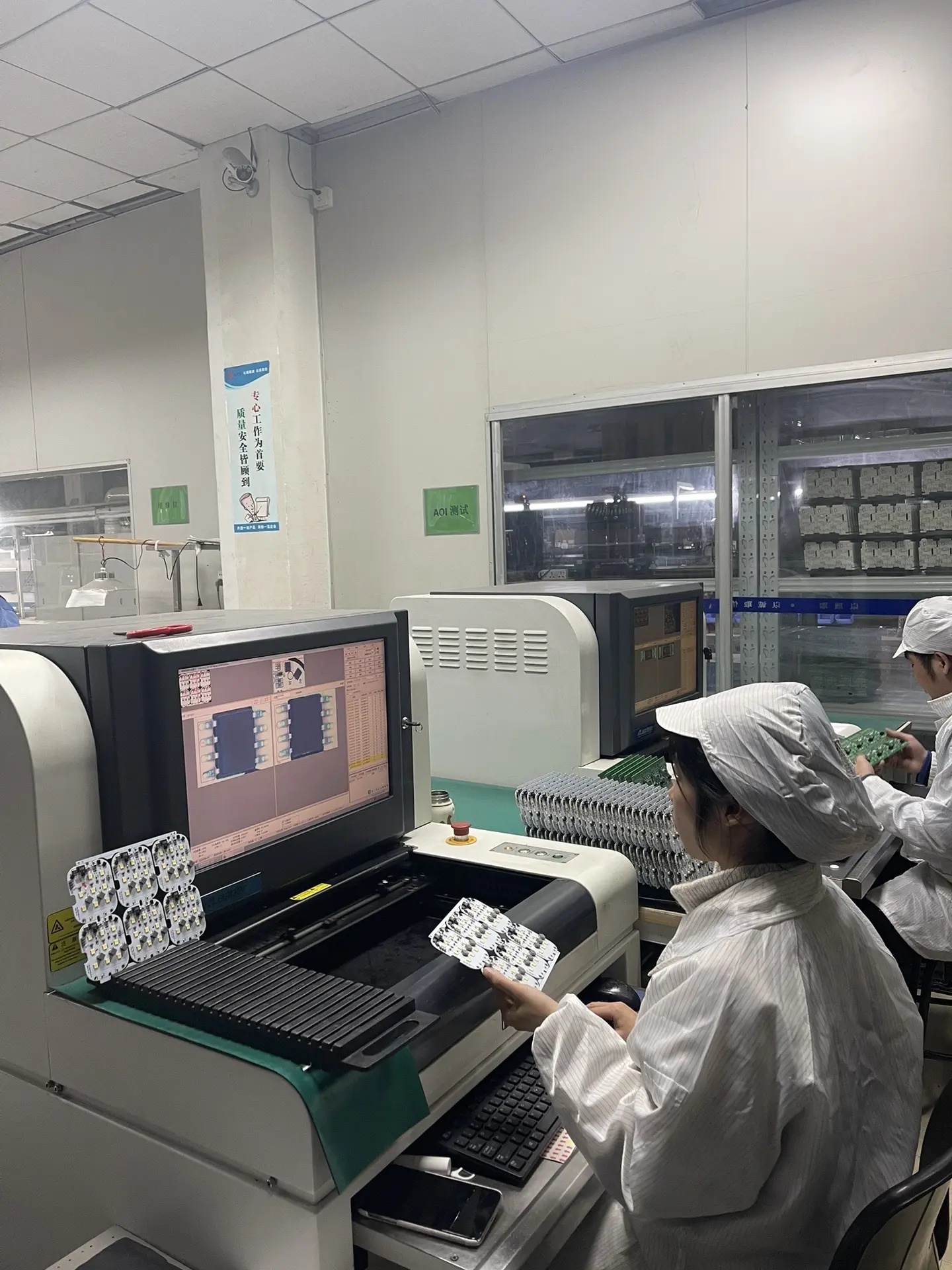
Inspection and Testing: Finally, the circuit board is inspected and tested to ensure that it meets design requirements and quality standards.This includes electrical performance testing, visual inspection, etc.
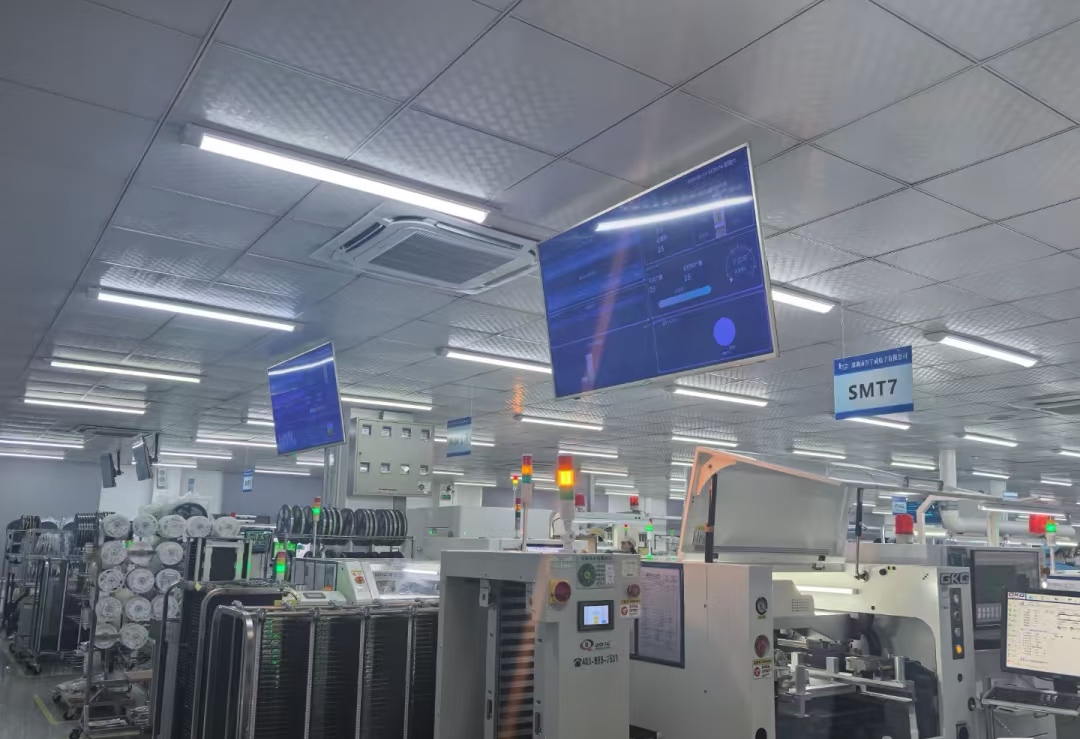
During the entire lamination process, attention should be paid to keeping the environment clean and controlling temperature and humidity to ensure the quality and production efficiency of the circuit board. At the same time, attention should also be paid to operating specifications and safety matters to avoid accidents.
10585 View